Originally posted by Bruno Putzeys in another thread
Well if you are very patient and have enough power devices to spend on failed amplifier you could just possibly get a UcD based ampliverter working.
Let's say I would not recommend it but just for the heck of it, here's how it could be done (mono amplifiers only):
1. Make a normal UcD loop.
2. Feed the comparator output to a state machine that alternatively switches the primary and secondary sides.
But here's the annoying bit:
3. Add a protection that will override the comparator output if it hasn't switched for the last few microseconds. Otherwise the primary side will blow instantly when the amp is clipped.
I'm not a fan of ampliverters though. The idea is very elegant, but the bilateral switches on the secondary side make things a bit more complicated in reality than in concept.
Hi,
Ampliverter is basically a transformer isolated class D amplifier, so it can be connected directly to the rectified mains voltage. Effectively it is just a SMPS with bidirectional synchronous rectifiers.
Compared to a classical class D amplifier it has some advantages (at least on paper):
- power supply is integrated, so it can be made small
- both pairs of switches operate at one half of the switching frequency, 200kHz in this case.
- there is no stored energy on the secondary, so DC speaker protection is not necessary.
- auxiliary supply voltages require only few turns windings on isolation transformer
I have read of only one commercial amplifier using this principle (Peavey). There are several patents on this topology, but the main one (US 4479175) has already expired. The most recent patents came from Nuforce (class N amps). All designs that I have seen use constant switching frequency and that seemed like a good idea at first. Only when I tried to close the feedback loop in simulation (using triangle derived from the secondary winding) I realized that delays in the modulator and driver chain produce DC offset at the output. I was then toying with PLL used as a modulator until I started to think about Bruno's idea. Variable frequency is not such a problem as it seems. At 200kHz transformer would operate at 0.05T because of the losses, so lowering primary frequency to 50kHz is no problem.
So here is a simulation of proof of concept UcD type ampliverter. It shows that the whole thing is not much more complicated than a commercial UcD amplifier which also incorporates current limiting, soft start and overvoltage protection. Simulation uses S elements as switches to speed up simulation, but i believe that all necessary parts are included. E elements with unity gain represent optocouplers or other digital isolators. Simulated circuit is stable into open and short circuit and is also protected against clipping. The whole concept of variable frequency ampliverter is not limited to the UcD type of modulator, it can also be used with leapfrog modulator or even self oscillating hysteresis modulator. Before I proceed with the final design I would like to know how much some second order effects can be detrimental to the performance of this circuit.
By second order effects I mean unmatched switching times in the primary and the secondary and unmatched delay from the modulator comparator to the primary and secondary switches. As can be seen from UcD vs ZapPulse thread switch transition times have far greater influence on distortion that I have originally thought. Any comments from Bruno, Lars, analogspiceman and all others are welcome. Also many thanks to Bruno for the original idea.
Best regards,
Jaka Racman
Attachments
Many thanks to you for this!
Seems like it'll work with mueta.. and possibly single cycle control?
It's been awhile since you've first mentioned ampliverter, great stuff.
Chris
Seems like it'll work with mueta.. and possibly single cycle control?
It's been awhile since you've first mentioned ampliverter, great stuff.
Chris
Hi Jaka, I like it! I am interested in taking this route since space is very scarce in my small living quarters. The concept of driving a speaker with a power supply has been attractive to me for quite a while. I first did it several years ago, but it was half class A, half class D.
I may have to wait until winter before I can really study the LTspice circuit. Thanks for providing it.
I may have to wait until winter before I can really study the LTspice circuit. Thanks for providing it.
Hi,
attached is leapfrog ampliverter LTspice file. Functionally, both leapfrog and UcD are equivalent (short, open and clipping protection). Leapfrog requires one comparator and three opamps, while UcD requires three comparators and one opamp. One possible advantage of UcD is comparator operating in inverting mode, so input common mode requirements are relaxed compared to the leapfrog where comparator requires large input common mode range. Also UcD has only one comparator in signal path, while leapfrog has three opamps and comparator. But UcD also uses opamp buffer input stage, so situation is still not very clear. I will probably have to try both solutions.
Chris, I think that single cycle control is only a complicated way of achieving advantages of hysteretic self oscillating design with constant frequency switching. I think that it it can be achieved more simply by adjusting hysteresis with input signal feedforward. Look at US5160896 for that.
Best regards,
Jaka Racman
Attachments
Hi Jaka,
I am glad to see you have been up to some serious fun with ampliverters and LTspice. 😀 The effort you clearly have put in deserves a response in kind. I just want to let you know that I have read your posts and plan to make a more serious response as soon as I can find the several hours it will require.
In the mean time here are a couple of quick comments:
I like how in the UcD-control based ampliverter you seem to have digitally ORed together voltage and current modes without the usual slewing delay glitches during mode transitions (leapfrog in inherently seamless in this regard).
It seems that because UcD control is closed around a second order filter (rather than a first order as in leapfrog), it suffers a kind of overshoot recovery glitch in the face of large amplitude steps (when the feedback loop is momentarily disconnected). Now that you've obviously played with both systems extensively, have you noticed a difference in this regard between UcD and leapfrog style control?
Regards -- analogspiceman
Hi analogspiceman,
I must admit that I have been more busy with the design of the state machine than by closing the loop. That's why I used published values in both UcD and leapfrog compensation circuits and threw in "educated guess" (first parts I had in the part's bin) 1k and 100pF value for the extra passive pole in the UcD compensatin circuit.
Yes, I have seen ringing in the UcD response, but hopefully it can be tamed, as actual UcD400 response shows.
I have now started to draw actual schematics. I will draw one for both the UcD and the leapfrog. As far as I can see, leapfrog my end up using even less parts, so I will probably try this one first. I am glad you will comment further, but please take your time.
Best regards,
Jaka Racman
Chris, I think that single cycle control is only a complicated way of achieving advantages of hysteretic self oscillating design with constant frequency switching.
Hi,
I think I can easily agree with that. I think I'd like to try out both ... just for some educational kicks.
To compare leap frog so directly with UCD.... hmmmm.
I don't consider that rendition of leap frog to be complete? It was only ever based off of the single ended "known from patent" version, and so the leap frog technique is of course single ended as well. You'd have to compare it to that same singled ended UCD.
The real UCD is of course fully differential, explaining the two input op amps, that it doesn't really need. I'd like to see a fully differential leap frog, I don't have a good enough grasp of the control loop to handle that one myself.
You also mentioned UCD driving into a short? It's not equivalent to leap frog in that respect, you need CMC for that right?
I think the ringing you're talking about is only tamed by limiting the input, somehow, like a LPF?
Regards,
Chris
PS:
Thanks again for contributing, these are the kinds of threads I really like!
This thing looks like a audio modulated smps to me.
That's exactly what an ampliverter is ! The idea is to get rid of one conversion process.
If we look at amps more generally then all of them are audio-modulated PSU's (most of them being post-regulator topologies).
Regards
Charles
Hi Chris,
yes I am now looking at the differential configuration of both modulators. With UcD, comparator now also sees common mode signal, so one advantage of UcD (in my list) has gone. On the other hand, by applying differential feedback on the leapfrog I was able to omit one inverting opamp.
My problem is that my background is SMPS. In SMPS, anything under 1% error is usually good enough, but not in audio. I am pretty much confident I can hack power stage together and close the feedback loop in a stable manner quick enough (been there, done that). But to go under 1% THD will require me to learn and experience new things, and this will take some time. I am getting a little old and I do not breadboard so fast as I used to. So I simulate more, but simulation is only good to grasp principle not to discover finesse. So by counting active devices I am trying to identify possible trouble spots. For instance, large common mode input range for comparator my force me to think about discrete design (I was intending to use IC, LT1394 for instance).
Best regards,
Jaka Racman
Hi Jaka,
Thank you for that reply.
You again bring up an excellent point. The common mode signal shouldnt' really be a problem... and apperently it isn't according to the performance of the actual modules.
Decent rejection is possible by using high precision components, the caps will degrade it at higher frequency but you can try to match those too. It seems to work great anyway.
So now is a good time to ask.... what's worse? Less CMRR or a non differential setup? I'm kind of leaning towards fully differential as being the better one, as always there's a little something we've got to give up for it.
Trust me I understand the problems with simulation.
Discrete design, certainly seems to be worth it in the long run, not exactly fun for prototyping though. It'll get you pretty good simulations though.
Looking forward to seeing how a differential version of LP measures up to the single ended one.
I'm trying to take a break from simulations for awhile (really I'm just sick of it) but when I get the urge again this thread is my first stop.
Regards,
Chris
Hi,
I'm sure the eventual reply will be well worth the wait 🙂
Have a good.. vacation?
Regards,
Chris
I'm sure the eventual reply will be well worth the wait 🙂
Have a good.. vacation?
Regards,
Chris
Hi,
attached are new LTspice versions of both UcD and LeapFrog ampliverter. Compared to the first version there are some improvements:
-differential construction like the real UcD
-startup is now reliable into any load from short to open with any offset voltage present at the input
-logic elements have been changed to reflect real components that will be used in the real design (74xx74 Dflipflop, 74xx02 NOR, 74xx86 XOR and ISL6207 gate driver)
-simulates faster
Best regards,
Jaka Racman
Attachments
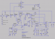
Hi,
attached is first revision of UcD type ampliverter schematic. I started with UcD type since I suspect it will be a little easier to debug than the leapfrog version. PCB is not yet finished. Here are some comments:
-primary (mains) part of the ampliverter is denoted by the light brown polygon. It should work independently of the secondary section and provide auxiliary supply voltages to the rest of the circuit. IC1 forms startup oscillator that works untill UcD modulator kicks in. It's oscillation frequency is set below lowest expected UcD modulation frequency under normal operating conditions.
-secondary part starts with a copy of the UcD modulator (from the published papers) comprising IC101 and IC102. Comparator IC102 should be LM361 or discrete design because of the rather high common mode signal at the input. Modulator's output is ORed with current limiting comparators IC104 and fed to both primary and secondary switching stage through toggle flipflops IC109.
-isolation of logic signals between the primary and the secondary circuit is achieved by HCPL-7723 optocouplers. This is potentially the weakest part of the circuit. Chosen optocouplers are pretty fast (16ns propagation delay and 1ns pulse width distortion typical), but if anyone knows a better alternative I would be grateful.
-both the primary and the secondary Mosfet drivers are transformer coupled, since under normal operating conditions both work with approx 50% duty cycle. Modulation is achieved by phase difference between the primary and the secondary, not PWM.
-main isolation transformer is divided into three identical transformers T1,T2,T3. This allows 1 to 1 turns ratio and reduction of the leakage inductance. Current sharing is automatic because of the series connected primaries. This also allows three sets of bidirectional connected Mosfets which switch only 1/3 of the total output current. Hopefully SO-8 devices will be used because of that.
Best regards,
Jaka Racman
Attachments
Originally posted by Jaka Racman
-secondary part starts with a copy of the UcD modulator (from the published papers) comprising IC101 and IC102. Comparator IC102 should be LM361 or discrete design because of the rather high common mode signal at the input. Modulator's output is ORed with current limiting comparators IC104 and fed to both primary and secondary switching stage through toggle flipflops IC109.
Digitally ORing together the voltage and current loops seems to avoid the usual mode-crossover problems that stem from excess charge accumulating on the inactive loop's compensation capacitor.
-isolation of logic signals between the primary and the secondary circuit is achieved by HCPL-7723 optocouplers. This is potentially the weakest part of the circuit. Chosen optocouplers are pretty fast (16ns propagation delay and 1ns pulse width distortion typical), but if anyone knows a better alternative I would be grateful.
A self oscillating amplifier requires a stable, controlled rate of change of phase to achieve controlled instability. Delay, if repeatable and not too large (like your 16ns optocoupler delay), can contribute nicely to this design function. Unless you know of another reason to further reduce this small delay, I wouldn't worry about it.
-both the primary and the secondary Mosfet drivers are transformer coupled, since under normal operating conditions both work with approx 50% duty cycle. Modulation is achieved by phase difference between the primary and the secondary, not PWM.
Always assume the worst sort of input signal will eventually appear. Imagine the largest possible input that is the highest possible subharmonic of the switching frequency. This type of input could drive the duty cycle to stray well away from fifty percent, leading a design that appears okay under normal audio full loading to fail due to transformer saturation.
-main isolation transformer is divided into three identical transformers T1, T2, T3. This allows 1 to 1 turns ratio and reduction of the leakage inductance. Current sharing is automatic because of the series connected primaries. This also allows three sets of bidirectional connected Mosfets which switch only 1/3 of the total output current. Hopefully SO-8 devices will be used because of that.
You are right that the transformer primaries must share the same current, but what ensures that they share the same voltage? Depending on the size of the interwinding capacitance, things might get especially dicey during the switching edges since the top transformer will be subjected to a three times greater voltage change.
However, my greatest concern with this design is that there is no provision for catching the current from the transformer leakage and output inductances during the inevitable on/off timing errors with the bilateral output switches. A friend of mine once built a working high power prototype ampliverter style sine wave power inverter. He found that the only practical solution to this problem was to clamp the troublesome nodes to catch capacitors (plus and minus) on the outputs and use small auxiliary power converter(s) to return the power to the input bus.
Regards -- analogspiceman
- Status
- Not open for further replies.
- Home
- Amplifiers
- Class D
- UcD ampliverter