We discuss not the "what would be the best to build" but "what would be the best to build for radio", assuming not too much of experience.
In the other thread I already recommended him to look at one of DX designs, destroyer x already came up with his suggestions.
Now, what's wrong with 50 years old design? 2 differential cascades with current mirror is highly linear, robust design in principle.
I design and build very new stuff, including non-standard CFA designs, however my VFA, based on Pioneer M3 Exclusive (1973) is an excellent amp I often use as a reference.
In which part DX Blame is newer than the 50 years old one?
The right one, symmetrical, simply has design problems - I already mentioned them in the other thread. It will not work properly as is. The left one will, even in the hands of not too experienced builder.
TO-3 - fully agree, I would not use them either.
We discuss not the "what would be the best to build" but "what would be the best to build for radio", assuming not too much of experience.
In the other thread I already recommended him to look at one of DX designs, destroyer x already came up with his suggestions.
Now, what's wrong with 50 years old design? 2 differential cascades with current mirror is highly linear, robust design in principle.
I design and build very new stuff, including non-standard CFA designs, however my VFA, based on Pioneer M3 Exclusive (1973) is an excellent amp I often use as a reference.
In which part DX Blame is newer than the 50 years old one?
The right one, symmetrical, simply has design problems - I already mentioned them in the other thread. It will not work properly as is. The left one will, even in the hands of not too experienced builder.
TO-3 - fully agree, I would not use them either.
Agree, we have to encourage people to discover new horizons😀 No more 50 years old designs.
How about it? Looks familiar? Have for more than 10 years. Enjoy very much, enjoy myself and all my neighbors.

Last edited:
The left one is hundred years old design. Nothing special about it. I always was wandering why people stick to old stuff ?? How you can say it is HI quality by looking at the schematic? =) It is so called Marshall design, 50 years old, nothing special, parameters depend purely on elements selection.
The right one, is the same. Pure symmetrical amplifier. Nothing special. Why bother make it? 2014 year outside the window.

Then as a comment on this Russian design Lazaro?😉🙂
thanks!!
Attachments
Last edited:
Please show this to the schematic.😕
thank you
See page 48, figure 56 of
http://www.sg-acoustics.ch/analogue_audio/power_amplifiers/pdf/audio_power_amp_design_comments.pdf
The question of compensation caps with double differential scheme has sometimes been raised in Wireless/Electronics World.
Then as a comment on this Russian design Lazaro?😉🙂
thanks!!
I am not a fun of symmetrical amps. No experience. I have the one that I posted above. The thing why chose it was damping factor. The author claims it to be 1000 in range of 5Hz..20kHz.
I am not a fun of symmetrical amps. No experience. I have the one that I posted above. The thing why chose it was damping factor. The author claims it to be 1000 in range of 5Hz..20kHz.
The author claims it to be 1000 in the range of 5 Hz .. 20kHz.
These are great features, but all the Russian transistors nowhere to be found.🙁:🙄
People I am for a simpler design audio amplifiers for home use, ...
To be specific: Which amplifier recommend this the first or the Russian Lanzaro?🙄
Or maybe this could come into consideration?🙁
thank you!
Attachments
Last edited:
Err, we have no 100 year old solid state designs. Transistors were not invented until the 50's.
For a first amp, why don't you build a GAINCLONE. Very high probability of success and a pretty darn good amp.
For a first amp, why don't you build a GAINCLONE. Very high probability of success and a pretty darn good amp.
Err, we have no 100 year old solid state designs. Transistors were not invented until the 50's.
For a first amp, why don't you build a GAINCLONE. Very high probability of success and a pretty darn good amp.
He will not build anything.
Err, we have no 100 year old solid state designs. Transistors were not invented until the 50's.
Wrong on both counts.
Then on 21 February 1906, L W Austen filed a patent for a tellurium-silicon detector. Then a month later in March 1906, General H H C Dunwoody in the USA patented a carborundum detector. This was followed by Greenleaf W Pickard filing a patent in August of that year for a silicon metal rectifier. This was the culmination of around four years work for Pickard who said he had been working on crystal detectors since 1902.
Crystal Detector
First LEDs:
Losov made some major advances and is a key person in the LED history. He undertook a considerable amount of work investigating light emission from Cat's Whisker style detectors. He observed and investigated the light emission from zinc oxide and silicon carbide crystal rectifiers.
As a result of his observations and investigations, Losov published a number of papers in the technical press of the day between 1924 and 1930. His first paper was entitled: "Luminous carborundum detector and detection crystals" which was published in a Russian journal.
LED History
First Transistor:
Lilienfeld’s construction appears simple, but the use of a solid compound opens in fact an avenue to solid-state devices. Similar to his idea with field-emission devices, where he totally left behind the classical thermionic diode or triode vacuum tube, he again thought about a different principle, now even more radical in thought, by focussing his undivided attention on the conductivity modulation of a solid by a transverse field. Starting 1926, in Brooklyn, N.Y., Lilienfeld applied for three patents.
The first two, from 1926 and 1928, describe what we now call a field-effect transistor (FET) structure. The first patent (J.E. Lilienfeld, Method and apparatus for controlling electric currents, US Patent 1,745,175, application filed October 8, 1926, granted January 18, 1930) gives a MESFET or metal/semiconductor FET. The second patent (J.E. Lilienfeld, Device for controlling electric current, US Patent 1,900,018 application filed March 28, 1928, patented March 7, 1933) is derived from the first, and gives a depletion mode MOSFET.
The n-type Metal – Oxide – Semiconductor Field – Effect – Transistor (nMOSFET) consists of a source and a drain, two highly conducting n-type semiconductor regions, which are isolated from the p-type substrate by reversed – biased p-n diodes.
A metal or poly – crystalline gate covers the region between source and drain. The gate is separated from the semiconductor by the gate oxide. The basic structure of an n-type MOSFET and the corresponding circuit symbol are shown in the Figure.
As can be seen on the figure the source and drain regions are identical. It is the applied voltages, which determine which n-type region provides the electrons and becomes the source, while the other n-type region collects the electrons and becomes the drain. The voltages applied to the drain and gate electrode as well as to the substrate by means of a back contact are referred to the source potential, as also indicated in the Figure.
The main technological problem was the control and reduction of the surface states at the interface between the oxide and the semiconductor. Initially it was only possible to deplete an existing n-type channel by applying a negative voltage to the gate. Such devices have a conducting channel between source and drain even when no gate voltage is applied and are called “depletion-mode” devices. A reduction of the surface states enabled the fabrication of devices, which do not have a conducting channel unless a positive voltage is applied. Such devices are referred to as “enhancement-mode” devices. The electrons at the oxide-semiconductor interface are concentrated in a thin (~10 nm thick) “inversion” layer. By now, most MOSFETs are “enhancement-mode” devices.
While a minimum requirement for amplification of electrical signals is power gain, one finds that a device with both voltage and current gain is a highly desirable circuit element. The MOSFET provides current and voltage gain yielding an output current into an external load which exceeds the input current and an output voltage across that external load which exceeds the input voltage.
The current gain capability of a Field-Effect-Transistor (FET) is easily explained by the fact that no gate current is required to maintain the inversion layer and the resulting current between drain and source. The device has therefore an infinite current gain in DC. The current gain is inversely proportional to the signal frequency, reaching unity current gain at the transit frequency. The voltage gain of the MOSFET is caused by the current saturation at higher drain-source voltages, so that a small drain-current variation can cause a large drain voltage variation.
The third patent (J.E. Lilienfeld, Amplifier for electric currents, US Patent 1,877,140, application filed December 8, 1928, granted September 13, 1932) describes two other transistor structures, the Metal Base Transistor or the Semiconductor/Metal Semiconductor Transistor (SMST) and the Schottky-Barrier-Collector Transistor or MSMT.
J.E. Lilienfield-US Patent 1,877,140. First known patent describing the Metal Base Transistor or the Semiconductor/Metal Semiconductor Transistor (SMST) and the Schottky-Barrier-Collector Transistor or MSMT.
--Julius Lilienfeld
 Lots of disrespect going here. One week bin time for anyone who continues. Note that this is an English language forum, and all bilingual posts (strongly discouraged) must be accompanied by a full translation. I recommend you desist from insulting each other in Macedonian.
You are right!
Thanks for the warning,
I would like to suggest to my friends to re create the layout
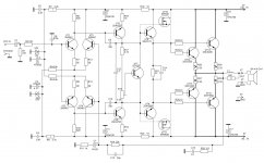
The schematic is Russian (look alike) and it is clever.... it is confused because the way was made.... too much informations, too much crowdy to let us understand easy.
This way, supported by better layout and more simulations, you may see the amplifier is not bad.
Maybe you did....i have not read the entire thread...go ahead folks...it is not a bad amplifier.
regards,
Carlos
Last edited:
- Status
- Not open for further replies.
- Home
- Amplifiers
- Solid State
- Two audio schematics-comment?!