Without any input signal and no feedback signal (which should be the case when the output stage is disabled) there should be no (or minimal) offset voltage at the output of the feedback amplifier. Especially when its DC gain isn't "infinite" like it is the case with your topology.
Could your Triangle generator be a source of DC offset voltage ? Or is it already AC coupled ?
Regards
Charles
Could your Triangle generator be a source of DC offset voltage ? Or is it already AC coupled ?
Regards
Charles
No, the offset (with very light or no load) is caused by the output stage itself. With both mosfets off, there is a floating negative voltage of more than -20V at the output, with high impedance, as it was easily nulled with a single potentiometer from +V rail to -V rail, the cursor connected at the mosfets midpoint. There must be some small unbalance in the mosfets off leakage current or perhaps something fed from the negative rail, as the driver, is producing that effect.
That produces a small DC offset at the input and it is amplified by the DC gain of the error opamp.
I traced the "problem" to be there, because as soon as I disconnect the feedback resistor there was no offset at the opamp.
However, this is IMHO not related to the turn on transient, as things are perfectly right when load is connected (I said, with below 500 ohm or so it starts perfect as the offset at the error amp is below the triangle amplitude, and with a "normal" (8 ohm for example), load, there was no appreciable offset at the error amp. output (at least with the o'scope)
So if there is no offset before enabling the driver and both driver circuits are powered up beforehand then there is only one cause for this transient I could imagine: The settling of the NFB loop. Do you still use the "little trick" that enhances phase-margin ?
But I don't know where the turn-off transient would come from. What is its amplitude ?
Regards
Charles
But I don't know where the turn-off transient would come from. What is its amplitude ?
Regards
Charles
Pierre said:No, the offset (with very light or no load) is caused by the output stage itself. With both mosfets off, there is a floating negative voltage of more than -20V at the output, with high impedance, as it was easily nulled with a single potentiometer from +V rail to -V rail, the cursor connected at the mosfets midpoint. There must be some small unbalance in the mosfets off leakage current or perhaps something fed from the negative rail, as the driver, is producing that effect.
That produces a small DC offset at the input and it is amplified by the DC gain of the error opamp.
I traced the "problem" to be there, because as soon as I disconnect the feedback resistor there was no offset at the opamp.
However, this is IMHO not related to the turn on transient, as things are perfectly right when load is connected (I said, with below 500 ohm or so it starts perfect as the offset at the error amp is below the triangle amplitude, and with a "normal" (8 ohm for example), load, there was no appreciable offset at the error amp. output (at least with the o'scope)
The 20 volts seen on the output is usually the difference between the negative rail and driver supply voltage. I trust you have something clamping the output to that level. I usually attach the high impedance pull down resistor to the lower driver's supply.
Have you made any changes yet? Still drawing the circuit out?
You NEED to precharge the bootstrap cap. The resistor and zener is good, worth doing a little researching on different ways of precharging, it gets a good mention in slup169 too. Nobody mentioned the extra diode. Bypass the zener with the 10n or whatever smaller value bootstrap bypass cap. Don't worry about bypassing the bootstrap cap itself.
If you add both resistors on either side of cap it will also shift the output voltage accordingly. You'll hear a little "thick" when you first plug it in with load attached if the precharge resistor value is too high.
You'll have to balance it all out with what works best, keept the resistors as high a value as you can get away and still have them do their job in the alloted time.
I really would change your error amp, if the 5532 has too much input offset to be DC coupled in the input stage of the Hypex modules I can't see how it would be any better for your application as an error amp, a wideband, low offset, precision op amp would serve best. DC offset will be compounded by unequal impedances at signal frequencies as well 🙂
You could try a 1pF cap across the inputs of it and see what happens?
Regards,
Chris
The schematics, as promised.
If something is clamping the output voltage down, it has high impedance. The only things I can think of are D3 or D4... but IMHO they shouldn't.
About precharge... I agree in that it should improve things, but it really didn't when I tried. I guess 1uF is low enough to have an almost unnoticeable effect as compared to other causes of the turn on "click".
Attachments
Nice circuit !
My imagination tells me that a high-side driver that is not ready (i.e. unpowered) at startup must lead to turn-on clicks, but my imagination might also be wrong.
One question: Why do you use a double comparator ? You could as well use one comparator and "phase-split" the drive signal just before your deadtime circuit (or use one of these sexy comparators with inverting and nonoinverting outputs).
Regards
Charles
Your imagination is, at least, logical.
If you are referring to the pre-charge circuit for the bootstrap capacitor, well, it seems to have something to do, as the "click" was reduced noticeably as soon as I reduced it from 10.1uF to 1.1uF (tantalum+ceramic caps).
But it is also true, as I have said, that adding a 30K resistor to VCC + zener in parallel) produced no improvement.
The delay from turn-on of the 12v_bias supply until the IR2113 SD pin is released is around 4 seconds (measured). (I think that the RC values shown are not correc now that I see it, it must be something like 100uF + 100k), so all should be estable by that moment, including the bootstrap cap charge.
Perhaps something related to the NFB network???
Hi Pierre
It looks as if your carrier is approx 6V p-p and 330 kHz. Your unity-gain frequency seems to be around 210 kHz from a short guess. This is too high. Didn't we once discuss this ? This could make your NFB loop settle less fast than optimal but it is not easy to predict how this would be perceived aurally.
Maybe the above is wrong and I would have to recalculate again.
Regards
Charles
Yes, Charles, you are right. In fact, sw freq. is around 290KHz.
In fact, I started with your recommended values, but then I played a bit experimentally and found best results with shown values. But perhaps I should rearrange it in order to have it theoretically correct: what mods do you suggest in order to low unity gain point?
In fact, I started with your recommended values, but then I played a bit experimentally and found best results with shown values. But perhaps I should rearrange it in order to have it theoretically correct: what mods do you suggest in order to low unity gain point?
Hi Pierre ,
I think you have Left Out one important thing that is : you haven't referenced the NON-inverting + pin of error amp with variable potential divider from bothrails to set the exact midpoint at output not simply an earth reference GND.
The rails should be from the Mosfet side that is + rail & - rail not + - 6.3 V types. This insures a small DC error correction always presented to the error amp....
Both SERGIO's as well as LT schematic Crest amp features this...
and I also have implemeted this...
The Complementary Comparator Scheme ,
I have implemented it before,
Charles you do remember this scheme which i proposed in one of my earlier threads and you helped me by giving your precious suggestions on using Differential Comparator LM360 instead , Thanks Once again Sir Charles Layman
regards,
K a n w a r🙂
I have also tried that, Workhorse.
In fact, adding a small DC correction at the input can lead to offset cancellation and hence make it start ok with very light loads. But as soon as you connect your real speaker, the DC correction needed produce an unnaceptable output offset (like 3V or so).
So unless you are right about the convenience of that adjustment, it doesn't help in this case.
Hi,
Kanwar that's a good tip, but you neglected to mention doing it for all op amp ground references as well, why not, they should all be common.
I'd run all those grounds to a single point I'm sure Pierre did anyway.
Pierre are Q1 and Q6 matched? How about their respected bias resistors? I could see a delay in one here possibly creating a DC offset once oscillation starts.
How about offset of the 319's? A read a small cap across the inputs can help with offset by making the noise common mode but am now sure how well that would work here.
I found window comparators were too sloppy for this kind of thing, but maybe you can couple your PWM outputs together and force them to keep up by linking them with a small cap or High value resistor, an RC snubber to control the slopes between the two could possibly be even better, they'll have to track the same slope you see? They're high impedance outputs so you should get away with it just fine.
Take Charles up on his advice and you can tighten up the slop from this area, think your problem will be solved.
Regards,
Chris
Charles...
I have just simulated my NFB scheme with the values shown in the posted schematics.
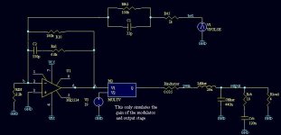
I am measuring open-loop response. Please tell me if I am doing it right: measure output/test_signal, where output is at speaker terminal, with 4-8 ohm load, and test_signal is a sine inserted just into the 1k resistor (R45), that is not connected to the mosfets anymore. Input terminal is shorted to GND.
Gain of the PWM stage is modelled by a fixed 19 V/V gain, calculated as the ration between supply rail and triangle peak amplitude (65V/3.5V, as a worst case, highest gain).
In that conditions, I obtain a 0dB loop gain point at 120KHz (8ohm load) and 98KHz (4ohm load). The initial phase is shown as 180degs, phase starts decreasing and at 0dB gain, phase is phase margin = 67 or 91º.
Is this procedure correct? (I attach curves for 4 ohm)
I have just simulated my NFB scheme with the values shown in the posted schematics.
I am measuring open-loop response. Please tell me if I am doing it right: measure output/test_signal, where output is at speaker terminal, with 4-8 ohm load, and test_signal is a sine inserted just into the 1k resistor (R45), that is not connected to the mosfets anymore. Input terminal is shorted to GND.
Gain of the PWM stage is modelled by a fixed 19 V/V gain, calculated as the ration between supply rail and triangle peak amplitude (65V/3.5V, as a worst case, highest gain).
In that conditions, I obtain a 0dB loop gain point at 120KHz (8ohm load) and 98KHz (4ohm load). The initial phase is shown as 180degs, phase starts decreasing and at 0dB gain, phase is phase margin = 67 or 91º.
Is this procedure correct? (I attach curves for 4 ohm)
Attachments

Hi Pierre,
The Level Shifter has something annoying criteria with it, you implement CE stage, but IMHO CB stage will perform better than it and of course it would be a little bit faster too and eradicate the delay problem associated with CE...
Have you tried to replace error amp with JFET input type TL072 opamp??
Since you have already inserted the deadtime before the gate driver IC then what is the purpose of again inserting at the gate drive of mosfets at the output, shouldn't it would increase T.H.D.
....
Hi Chris,
I think the Error opamp is the one who controls the offset upto maximum extent than another device in this circuit...
Secondly ,The Window Comparators inturn causes some Deadtime between complementary PWM outputs, this may be adjusted by using simple resistors at input of Comparators and also the triangle input should be well isolated with a capacitor to eliminate any DC offset entering the Window Comparators...
regards,
K a n w a r
The Level Shifter has something annoying criteria with it, you implement CE stage, but IMHO CB stage will perform better than it and of course it would be a little bit faster too and eradicate the delay problem associated with CE...
Have you tried to replace error amp with JFET input type TL072 opamp??
Since you have already inserted the deadtime before the gate driver IC then what is the purpose of again inserting at the gate drive of mosfets at the output, shouldn't it would increase T.H.D.
....
Kanwar that's a good tip, but you neglected to mention doing it for all op amp ground references as well, why not, they should all be common.
Hi Chris,
I think the Error opamp is the one who controls the offset upto maximum extent than another device in this circuit...
Secondly ,The Window Comparators inturn causes some Deadtime between complementary PWM outputs, this may be adjusted by using simple resistors at input of Comparators and also the triangle input should be well isolated with a capacitor to eliminate any DC offset entering the Window Comparators...
regards,
K a n w a r
Thanks for all the tips!
- I did try with a TL082 (jfet input) with exactly the same results.
- About level shifting, in fact I also tried CB configuration and noticed no improvement in speed, in fact these are working quite well and fast ;-)
- About dead-time: perhaps there is a bit too much deadtime resulting from the addition of the input caps (I think it works equally well with them removed, IR2113's input capacitance being enough) and the diode in the gates. However, that diode also helps in speeding turn-off up.
- About the comparator: I also tried AD8561 and TL3016 with no improvement in speed (in fact very small improvement, totally voided by the level shifters) so I decided to use LM319 for cost reasons.
- About offset: in fact, the circuit, as it is now, produces very low output offset, I would say less than 50mV, with no correction. I am quite happy with that!
Chris, I am not sure if I understand you very well when you talk about coupling comparators outputs together . What's the purpose and expected improvement?
Thanks!
Workhorse said:Hi Pierre,
The Level Shifter has something annoying criteria with it, you implement CE stage, but IMHO CB stage will perform better than it and of course it would be a little bit faster too and eradicate the delay problem associated with CE...
Have you tried to replace error amp with JFET input type TL072 opamp??
Since you have already inserted the deadtime before the gate driver IC then what is the purpose of again inserting at the gate drive of mosfets at the output, shouldn't it would increase T.H.D.
....
Hi Chris,
I think the Error opamp is the one who controls the offset upto maximum extent than another device in this circuit...
Secondly ,The Window Comparators inturn causes some Deadtime between complementary PWM outputs, this may be adjusted by using simple resistors at input of Comparators and also the triangle input should be well isolated with a capacitor to eliminate any DC offset entering the Window Comparators...
regards,
K a n w a r
It does but in his design the reference is not AC coupled like you're saying so it's critical all those grounds are common and tight, precision components etc, referenced to the rails virtually like you're saying. AC coupling is easier and a good idea.
I'm not sure is resistors is at the comp. inputs and AC coupling the reference signal will be enough to cure this given the independant pwm outputs.
With drift and component variation while a resistor at the input may adjust the deadtime statically it won't do much to ensure that Q1 and 6 work in tandem and stay that way.
The gate resistor is a requirement to decouple it from the driver. This will help the driver by sharing power consumption and dampen parasitic ringing. Could also help limit EMI by slowing turn on and in extending the Vds slope to allow for recombination in the body diode. It could either hurt THD or help it, the right value shouldnt' hurt it.
Regards,
Chris
Salut Pierre
Your open-loop bode plot doesn't look bad indeed. I'd leave it like that - even more when these are TRIED values.
My gut feeling is still that it must be some sort of offset that needs to stabilise. As Chris and Kanwar mentioned we should not forget inaccuracy in the time-domain as a possible source of offset.
Since you use two comparators, one could also implement some kind of soft-start.
Regards
Charles
Thanks, Charles.
I am glad that the open-loop response looks good to you, but is the model and the way of measuring it correct? I would like to settle this solidly so I (and others) can have a good tool to analyse the feedback networks.
Mmmm. Your idea about soft-start is good and I have also though about that if you mean that the volume (gain) increases slowly when the circuit starts.
But the problem is... how can I implement that? I really don't see it easy using the comparators, do you have any particular idea that want to share with us?
One test that is very easy for me is AC coupling the triangle to the comparators. When I have done it I will tell you the results.
Best regards,
Pierre
Pierre the very small valued cap across comp. inputs is said to neutralize the DC offset/drift by keeping fast acting transients/noise common to both pins so that the op amp /comparator may reject it. I've only seen a few pico used her, nothing more. It's a bandaid. I'm just throwing ideas your way though.
Here's another one I forgot to mention earlier. Still picking on Q1 and 6. Those are high voltage/current medium power video amplifier/switches.
They work, but I don't think best. Consider trying a low voltage small signal with high Beta and Ft. Something like a 2N3904 is a good candidate IMHO. I think you'll get cleaner and faster signals to your driver that way.
Regards,
Chris
- Status
- Not open for further replies.
- Home
- Amplifiers
- Class D
- Turn on/off transients