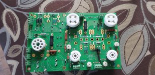
So I finished building my TSE ii today and am having multiple issues with the checkout procedure. Any help at all would be greatly appreciated! So now for the issues:
-upon inital powerup, it ran for a few seconds and then there was a flash and smoke. I immediately turned the power off and found a burned mark between d2 and d3 on the bottom side of the board (see pic). I looked and did not see any solder bridge between the two nor was there any visual damage to either diode. This event also blew the fuse. I cleaned up the burned area and did not notice any other damage. I tested both diodes, both show .5v and only pass voltage one direction.
- I then replaced the fuse and tried powering up again. I am getting the following measurements with no tubes installed and have no clue where to start on the troubleshooting:
B+ 0v
B- -174v
rect heater volt 0v
300b heater volt 4.98v
5482 heater volt 8.3v
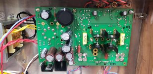
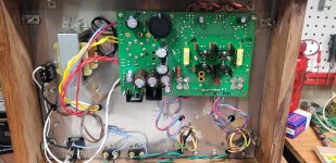
I have uploaded a few pictures of the build. Thanks again.
Bryce
-upon inital powerup, it ran for a few seconds and then there was a flash and smoke. I immediately turned the power off and found a burned mark between d2 and d3 on the bottom side of the board (see pic). I looked and did not see any solder bridge between the two nor was there any visual damage to either diode. This event also blew the fuse. I cleaned up the burned area and did not notice any other damage. I tested both diodes, both show .5v and only pass voltage one direction.
- I then replaced the fuse and tried powering up again. I am getting the following measurements with no tubes installed and have no clue where to start on the troubleshooting:
B+ 0v
B- -174v
rect heater volt 0v
300b heater volt 4.98v
5482 heater volt 8.3v
I have uploaded a few pictures of the build. Thanks again.
Bryce
Attachments
Last edited:
Here's a copy of the schematic another forum member made. It doesn't make sense that you have negative voltage if you saw lightning between the two diodes D2 and D3?
Also, I'm not sure what type power transformer you're using? Are your wires connected correctly? I seem to recall that not all the capacitors are needed for certain tubes?
Check out this thread for some possible help with your amp:
Tubelab SE-II Checkout
Also, I'm not sure what type power transformer you're using? Are your wires connected correctly? I seem to recall that not all the capacitors are needed for certain tubes?
Check out this thread for some possible help with your amp:
Tubelab SE-II Checkout
Attachments
Also, check the thread regarding the TSE must die: (I think it should be renamed the TSE WON'T DIE)
After a 14 year run, the TSE must DIE!
After a 14 year run, the TSE must DIE!
Here's a copy of the schematic another forum member made. It doesn't make sense that you have negative voltage if you saw lightning between the two diodes D2 and D3?
Also, I'm not sure what type power transformer you're using? Are your wires connected correctly? I seem to recall that not all the capacitors are needed for certain tubes?
Check out this thread for some possible help with your amp:
Tubelab SE-II Checkout
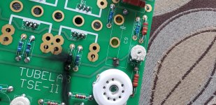
I am running an edcor xpwr 178 transformer and i tripple checked my wiring. I attached a pic of the wiring colors as well.
Ive looked through the schematic and it makes no sense that im not getting voltage to the rectifier as its the first thing fed out of the transformer. I dont understand how the power tubes are getting 5v without 5v at the rect heater
Attachments
Last edited:
Hi Bryce,
Things might not be as bad as you think. It sounds like you're following the checkout procedure ok, and listing the voltages is a good start.
First, the burned area shown in the picture is dead evidence to me of a short. If a solder bridge was the cause then it probably disappeared in a ball of plasma. It's good that you cleaned the traces, but look closely and make sure there isn't any damage to the board (e.g. cooked traces, fraying fiberglass substrate, etc.). I know you said you checked, but a second look never hurts.
Now for the voltages. How and where exactly were they measured? It makes a difference, and they could be OK depending. For instance:
Anyway, it looks like you're almost there. Just be patient, check your work, and skull it out. You'll get it. 🙂
Things might not be as bad as you think. It sounds like you're following the checkout procedure ok, and listing the voltages is a good start.
First, the burned area shown in the picture is dead evidence to me of a short. If a solder bridge was the cause then it probably disappeared in a ball of plasma. It's good that you cleaned the traces, but look closely and make sure there isn't any damage to the board (e.g. cooked traces, fraying fiberglass substrate, etc.). I know you said you checked, but a second look never hurts.
It makes perfect sense if you think about it; they're derived from two separate heater windings. The 4.98 V you're reading for the 300Bs is regulated DC derived from the 6.3 V transformer winding (the brown/brown-white wires). The 5 V for the rectifier is AC, fed by the transformer's rectifier winding (the yellow wires).I dont understand how the power tubes are getting 5v without 5v at the rect heater
Now for the voltages. How and where exactly were they measured? It makes a difference, and they could be OK depending. For instance:
- B+ 0v - This is absolutely normal if you're measuring this at pin 2 of the 300B sockets and the rectifier tube isn't installed.
- B- -174v - This isn't normal if measured at pin 3 of the 300B socket. According to George you should be able to adjust this from about -35 to -100 volts. Could it be that you're reading the plate voltage for the 5842s instead? That -174 V looks suspiciously close to the 175 V CCS voltage, but with the meter leads reversed (I know because I've done this myself).
- rect heater volt 0v - Was this measured between pins 2 and 7 of the rectifier socket? If so, then measure the 5 V wires where they enter the board.
- 300b heater volt 4.98v - This is normal, and evidence that the 6.3 V transformer winding is wired and jumpered correctly.
- 5482 heater volt 8.3v - Also completely normal when the 5842s aren't installed. This is because the circuit is unloaded; it'll settle down to 6.3 VDC when the tubes are in place. Incidentally, these heaters are fed from the same transformer winding as the 300Bs (it's just a branch circuit).
Anyway, it looks like you're almost there. Just be patient, check your work, and skull it out. You'll get it. 🙂
Hi Bryce,
Things might not be as bad as you think. It sounds like you're following the checkout procedure ok, and listing the voltages is a good start.
First, the burned area shown in the picture is dead evidence to me of a short. If a solder bridge was the cause then it probably disappeared in a ball of plasma. It's good that you cleaned the traces, but look closely and make sure there isn't any damage to the board (e.g. cooked traces, fraying fiberglass substrate, etc.). I know you said you checked, but a second look never hurts.
It makes perfect sense if you think about it; they're derived from two separate heater windings. The 4.98 V you're reading for the 300Bs is regulated DC derived from the 6.3 V transformer winding (the brown/brown-white wires). The 5 V for the rectifier is AC, fed by the transformer's rectifier winding (the yellow wires).
Now for the voltages. How and where exactly were they measured? It makes a difference, and they could be OK depending. For instance:
Also, what's the purpose of the blue wire in the upper left-hand side? It looks like it's soldered to the pad adjoining the one for the HV center tap, but I can't tell. A picture of the other side of the board might help, too.
- B+ 0v - This is absolutely normal if you're measuring this at pin 2 of the 300B sockets and the rectifier tube isn't installed.
- B- -174v - This isn't normal if measured at pin 3 of the 300B socket. According to George you should be able to adjust this from about -35 to -100 volts. Could it be that you're reading the plate voltage for the 5842s instead? That -174 V looks suspiciously close to the 175 V CCS voltage, but with the meter leads reversed (I know because I've done this myself).
- rect heater volt 0v - Was this measured between pins 2 and 7 of the rectifier socket? If so, then measure the 5 V wires where they enter the board.
- 300b heater volt 4.98v - This is normal, and evidence that the 6.3 V transformer winding is wired and jumpered correctly.
- 5482 heater volt 8.3v - Also completely normal when the 5842s aren't installed. This is because the circuit is unloaded; it'll settle down to 6.3 VDC when the tubes are in place. Incidentally, these heaters are fed from the same transformer winding as the 300Bs (it's just a branch circuit).
Anyway, it looks like you're almost there. Just be patient, check your work, and skull it out. You'll get it. 🙂
Thanks a ton for the help. I got back into it this morning and made some progress and then it really all fell apart...
First to answer your questions:
I was measuring B- at r6. The blue wire connected to the board is tied into the star ground on the chassis which is also connected to the iec ground and the speaker terminal grounds.
So Ill start with the good news I guess. I double checked everything and all looked well. No solder bridges anywhere on the board and no other obvious physical damage. I disconnected the 6.3v center tap from the board and started the checkout procedure again. This time all the heater voltages were looking good so I proceeded to throw the rectifier tube in and continue. This is when it quickly got ugly.
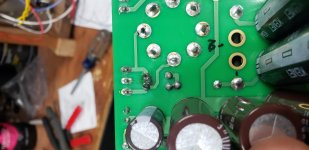
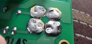
While monitoring B+ and voltages at each output tube, I turned the power back on with the rect installed. After a few seconds of the tube heating up, I began to show B+ increasing as expected. Maybe 5 seconds after B+ started climbing, I started getting a short between pins 1 and 2 (of the outermost power tube) on the bottom side of the board). I immediately shut the power down. I had closely checked this area multiple times for solder bridging because I was concerned with the close proximity of the traces. I can say with certainty that there was no solder between these two pads as I had checked it multiples times. I attempted to clean the damaged area and found that it had burned through quite a bit of the board and left a gap in the board.
I then started the board back up, keeping a close eye on the area, and all seemed well for about 15 seconds and then it got real interesting. There was a ton of arcing and smoke from the top of the board and I killed the power. Pulling the board revealed the following: r17 was completely smoked and splattered around the board. The bottom pad of C9 appears to have shorted to the trace of r12 which runs directly above it. the solder from r19 appears to have melted and splattered onto the connecter just below it. I think that about sums up the visible damages.
Any idea what could have caused all this damage to occur at the same time? Is it safe to assume that this board is ready for the trash and it would be best to start from scratch? I have to admit, I thought the chassis would be the hard part of the build but that doesnt appear to be the case. Feeling more than a little frustrated at the moment but still want to get this project completed.
Thanks again for the help.
Attachments
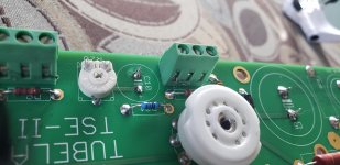
Being that R16 and R17 look real crispy, I would check IC1 and IC2. In one of your photos, it looks like the two fasteners may be touching or are really too close. If there's no plastic washer and/or mica insulator, there could be current flowing between IC2 and IC1.
The bolts are very close (probably a few mm) however I have the insulator and plastic washer on the bolt so there shouldn't be any voltage on the bolt itself.Being that R16 and R17 look real crispy, I would check IC1 and IC2. In one of your photos, it looks like the two fasteners may be touching or are really too close. If there's no plastic washer and/or mica insulator, there could be current flowing between IC2 and IC1.
I'm not familiar at all with the new board, but R17 clearly had a lot of current through it. If the 5842 was not in the socket, I don't see how current can go anywhere through R17 unless C9 was shorted.
Those are impressive burn marks ( burn marks are not necessarily a badge of shame on this sub forum ), but if the trace(s) involved are still intact, or can be replaced by a wire jumper, I wouldn't see a need to get a new board - yet. If you don't know what mistakes were made on this one, you might make the same mistake over again on a new board and be back where you started. Once you debug this one, and if the burn marks bother you, then maybe a new board.
Clearly, you need to find out what is wrong here. You are using both sides of the board, is it possible you have not got the MOSFET's or 10M45's oriented correctly?
I would guess you would start at the basics - don't panic, look at each component closely; make sure it is the correct component for that location, it is oriented correctly, and test it's value if you can. You may want to remove the MOSFETS and 10M45's and make sure they have no gone to short in all this drama.
but R17 clearly had a lot of current through it....the solder from r19 appears to have melted and splattered onto the connecter just below it
R19 is the input to ground resistor. It carries ZERO current. There are too many things here that don't make sense, yet all of the pictures seem to show a correctly assembled board with correct off board wiring.
For 300B's make sure NOT to connect the 6.3V CT. In your photo it looks like it is.
Connecting the CT to the board is OK, as long as the jumpers are in the proper places (they are) the CT will not be used.
Something is causing a LOT of current to flow in places where it shouldn't. I have studied all the pictures and can only think of one thing right off hand.....
What kind of solder was used to build this board. Was something with an acid core, or other non electronic solder used like plumbers solder? Please post a picture of what you used. These pictures seem to indicate some sort of conductive residue around the solder joints that flashed over in the presence of high voltage.
I'm not familiar at all with the new board, but R17 clearly had a lot of current through it. If the 5842 was not in the socket, I don't see how current can go anywhere through R17 unless C9 was shorted.
Those are impressive burn marks ( burn marks are not necessarily a badge of shame on this sub forum ), but if the trace(s) involved are still intact, or can be replaced by a wire jumper, I wouldn't see a need to get a new board - yet. If you don't know what mistakes were made on this one, you might make the same mistake over again on a new board and be back where you started. Once you debug this one, and if the burn marks bother you, then maybe a new board.
Clearly, you need to find out what is wrong here. You are using both sides of the board, is it possible you have not got the MOSFET's or 10M45's oriented correctly?
I would guess you would start at the basics - don't panic, look at each component closely; make sure it is the correct component for that location, it is oriented correctly, and test it's value if you can. You may want to remove the MOSFETS and 10M45's and make sure they have no gone to short in all this drama.
The MOSFET being mounted incorrectly is a possibility. I copied the orientation that George shows on page 26 of the tseii thread and all matches up.
Im wondering if the burnt trace from r12 which shorted to c9 is what ultimately caused r17 to blow.
Can small amounts of leftover flux on the board cause shorts like Ive seen? I did a less than stellar job cleaning up the flux after assembling the board.
R19 is the input to ground resistor. It carries ZERO current. There are too many things here that don't make sense, yet all of the pictures seem to show a correctly assembled board with correct off board wiring.
Connecting the CT to the board is OK, as long as the jumpers are in the proper places (they are) the CT will not be used.
Something is causing a LOT of current to flow in places where it shouldn't. I have studied all the pictures and can only think of one thing right off hand.....
What kind of solder was used to build this board. Was something with an acid core, or other non electronic solder used like plumbers solder? Please post a picture of what you used. These pictures seem to indicate some sort of conductive residue around the solder joints that flashed over in the presence of high voltage.
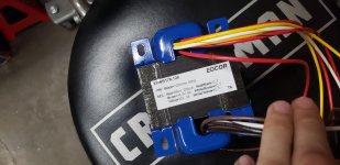
Thanks for the reply George. Here is the solder that I am using.
SMDSW.031 4oz Chip Quik | Mouser
… Can small amounts of leftover flux on the board cause shorts like Ive seen? I did a less than stellar job cleaning up the flux after assembling the board ...
Well, I wouldn't think so. I never bother with cleaning up a board after I've built it. When they get really grungy, they may get cleaned in the dishwasher, but that can be years, even decades, after they were assembled …
Your solder choice looks ok to me, although lately I've been using the stuff from Radio Shack that has a bit of silver in it, and I really like that.
Your solder choice looks ok to me
I don't see an obvious issue, but I have never used or seen that stuff before.....I stockpiled a lifetime supply of 1980's vintage Alpha and Kester solder at the Dayton hamfest a couple years back.
using the stuff from Radio Shack
You still have a Radio Shack store? Ours turned into a Sprint store and tried to sell Sprint phones.....Sprint has no coverage here, so that didn't work out well. I thing there is a vaping store there now.
... You still have a Radio Shack store? ...
There is one dealer store left in Fayetteville, almost halfway between our two residences, which is really a pretty good store - it's a college town, in the same place as when I was in school there; lots of raspberry pi / arduino / adafruit stuff, and other stuff that EE students might use, besides Radio Shack brand items.
I'm apparently the only person in the ham community around here that builds, and every once in a while I'll find a sack of parts or stuff at the back door to the office. One had 4 new rolls of this Radio Shack silver solder and it's really pretty good stuff. Made the SMD work a LOT easier.
Well I ordered a new board and components to assemble it. Between the large burned open gap between the power tube pads and the other damage from exploding components, I don't feel like its worth too much of my time or effort to keep messing with this board. I would hate to kill a $100+ transformer trying to troubleshoot a component that is showing not easily explained behavior.
I will get the board built when it arrives and hopefully have better luck the second time around. I also ordered some different solder (radioshack w the silver) just to rule it out as a possible cause.
If anyone else has any thoughts on what may have been causing my issues please feel free to chime in as I hate not knowing why stuff isn't working correctly and I am clearly far beyond my knowledge base on this one.
Thanks
If anyone else has any thoughts on what may have been causing my issues
I sent you an email a couple of hours ago. I am also quite curious as to what happened since everything appears to have been built right.
I sent you an email a couple of hours ago. I am also quite curious as to what happened since everything appears to have been built right.
Just saw your email a few minutes ago and send you a reply.
- Home
- More Vendors...
- Tubelab
- TSE II checkout issues help needed