How can the shape of a digital transmitted wave (square) have any effect on the sound, if said wave sahpe does not have serious signal integrity issues. Ie the data sent and data recieved match (bit perfect). This is what digital does, it is very tolerant of noise and other issues that can seriously upset analogue signals.
But a crappy looking square wave (99% when looked at with a scope that has the bandwith for todays square wave harmonic content) will not sound different from a nice clean square wave. The main thing is to have a monotonic rising and falling edge to the wave.
But a crappy looking square wave (99% when looked at with a scope that has the bandwith for todays square wave harmonic content) will not sound different from a nice clean square wave. The main thing is to have a monotonic rising and falling edge to the wave.
The shape of the square wave can affect the switching point in the receiver data slicer, and so introduce jitter. If you are just transmitting data this has no effect, but digital audio SPDIF also uses the data stream transitions to set timing. The receiver PLL will remove most of the jitter, but it is obviously better not to introduce jitter in the first case.
A "crappy" square wave may sound worse than a clean square wave - it all depends on what effect it has on the data slicer threshold voltage.
A "crappy" square wave may sound worse than a clean square wave - it all depends on what effect it has on the data slicer threshold voltage.
You know that a TTL/CMOS buffer/inverter with several gates in parallel does the same job? For example, SN74ACT04 can drive 24mA on each of the outputs... Sufficient for 75 ohm / 1Vpp. As for "better square" see below...Guys, the answer is easy:
BUILD the thing-a handful of parts, a few mintes of soldering.
After all, the site shows scope traces that show better square wave performance vs stock.
True. The only thing that metters are the transitions - they need to be precise and fast.A "crappy" square wave may sound worse than a clean square wave - it all depends on what effect it has on the data slicer threshold voltage.
The signals in the link that started this, are irrelevant in this aspect, he is looking only to get "flat" signals, which means nothing in the end.
Last edited:
If your slopes are correct the shape of the rest of the wave shape wont matter, it is getting the rising edge and falling edge, clean with no switch back on those edges, that will give you the desired results, as I said. the top of the wave can look like a complete mess, it will not affect the sound if the switching points are looked after (rising and falling edges). We recently hired a 13GHz scope as we had a DDR3 problem, and while we had it looked at a lot of different waves forms. What lookes clean on even a 4G scope looked horrendus. We use our signal integrity tools to make shure the switching edges are clean and the rest follows, if those edges stat getting messy most digital systems will fall down. Even the simplest of systems and signals look worse the better your scope is, and we were suprised that how nasty some look. The choice of driver and its drive capabilities also has a big effect, with some of the cheeper simpler 74 buffer devices producing better results than some fancy specificly designed buffer chips.
We have also found that layout with even the simplest signal and impedance matching are critical to the wave form results.
So as I said earlier if you look after the switching edges, the rest doent matter that much.
We have also found that layout with even the simplest signal and impedance matching are critical to the wave form results.
So as I said earlier if you look after the switching edges, the rest doent matter that much.
Great stuff marce, can you recommend a good 74 buffer for distributing a clock (16.xx) in a DAC?
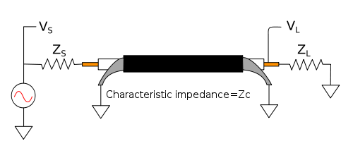
Also, what sort of series termination values would you use for audio digital? 47R, 51R?
Should that termination be at the source or destination chip in a digital transmission line?
You should look up the work of Pete Goudreau on rec.audio who modified an Assemblage DAC and in his evaluation it ended sounding like a much more expensive commercial DAC (Mark Levinson IIRC)
The "impedance matching" should be done at both ends... If you ask about the receiving impedance, that should be put at the end of the line.
This may be because they have slower transitions, so there is less HF energy to get reflected. Remember, the harder you look the more you will see. A sharp transition 'probes' the transmission line and terminations at higher frequencies, and may show up issues which are of no consequence at all for the desired purpose. (Like some square wave testing of amplifiers).marce said:simpler 74 buffer devices producing better results than some fancy specificly designed buffer chips.
Let's say you bought a second-hand book, and wanted to examine its condition. You would probably just use your eyes. You might use a magnifying glass. You would probably be daft to use a microscope, as all books look rough under a microscope.
Dr H, we have used LVT244 from Ti and NXP and the CDCV304PWR clock buffer chip from Ti.
DF96, when you look at the output curves for the 74 buffers, they seem to have a more solid drive (and a more linear curve). A lot of our designs use DDR3, gigabit ethernet, and other high speed interfaces as well as lower speed and audio (we do vehicle communication equipement for some very demanding customers). With all the different device core voltages we have numerous point of load switch mode power supplies etc so have numerous design issues to overcome, not only signal integrity but also EMC compatability, where again we have to go above and beyond normal commercial levels.
One SI problem we had was a 16MHz clock to some Ti codecs, one of the slowest clocks on the board! Yes a 13G scope is required for the fast interfaces, but while we had the tool it was useful to be able to see what artefacts were present on slower signals and where they came from, and yes some of them were not causing problems, but it is educational to see how the waves realy look. This helps us better equate them to Si software output that shows every gremlin on a waveform. Looking at the signals with more sober scopes give a much prettier picture, ie square waves, but for us we are having to go to such levels because of our products and to avoid any possible problems.
We also have to cope and try and eliminate the noise from cascaded SMPS. I miss the simpler days of PCB layout when it was just joining the dots, but find the new challanges and re-education I am going through is putting some excitement back in my life.
I guess at 13GHz you have to be very careful how you attach the scope - do the probes have a buffer in them? Your work makes SPDIF look like child's play, except for the fact that it is providing timing as well as data.
Hi DF96,
DDR memory is appearing in everything, as it is the most readily available and quite often the only option.
Even with our basic scopes (Tektronix DPO4034) we have to be careful with the scope probes, mainly the length of the ground lead. And have to model the scope leads in the Signal Integrity software, as this document illustrates:
TekConnect™ Probes: Signal Fidelity Issues and Modeling > Application Notes and Technical Documents : Tektronix
And when you start using 13G scopes the probe manual is 180+ pages!
http://www.home.agilent.com/upload/cmc_upload/All/01169-97011.pdf?&cc=GB&lc=eng
What we have learned is that at any speed and with any probe, loading of the signal is going to happen, so you have to cater for that in what you see. This probe loading can sometimes make a signal better than it is, we had an interface that worked when the JTAG clock was probed, but stopped working when the probe was removed.
The data speeds we and many others work at are pretty standard for a lot of digital stuff, every PC has ddr memory, note books tablets, I have even done phones with DDR ram interface! But even basic digital designs are becoming more complex due to the ever decreasing signal rise times.
As I said earlier, we often have mode problems with lower speed interfaces, especialy ones based on Manchester encoding such as SPDIF, as a lot of the newer faster interfaces emply LVDS, if not on all lines, then on the critical ones such as clock signals. Whereas older interfaces are still single-ended or as you stated clock and data together in SPDIF
The attached PDF wave shows a screen shot from the SI software, this was the signal that adding a probe into the circuit removed the switch back (non-monotonicity) from the rising and falling edges and also squared the waveform up, this is a 12MHz clock going to 4 inputs, routed as a daisy chain.
The PDF wave2 shows the same driver and basic circuitry, but with a buffer between the driver and the recievers, while the wave looks worse , it performs better as the rising and falling edges have no switch back, so there is less chance of false triggering. The ringing is due to the clock drives strong output, some ac paralel termination at the buffer input would reduce this.
Its good fun doing signal integrity, the main difference between this and spice moddeling is that this takes into account the physical aspect of the layout, routes, ground planes, track impedences etc. The use of these tools is becoming more common place as design respins become very expensive, especialy when you have 12-18 layers in a PCB design.
Attachments
My 2 cents: The best probe that I had was a 10:1 compensated probe.
The "direct" 1:1 probe was almost always changing the signal due to supplementary capacitive load added to the circuit.
The "direct" 1:1 probe was almost always changing the signal due to supplementary capacitive load added to the circuit.
- Status
- Not open for further replies.
- Home
- Source & Line
- Digital Source
- TRubes and JFETS as SPDIF drivers/buffers?