Hi, I'm an Electrical Engineering college student and I just finished designing and building my first amplifier. It's a 3 stage BJT amp, although of note is that we ran out of PNP power transistors so I had to use a quasi-complementary output stage. Anyway, my problem is that the simulation works perfectly (for my requirements) and I built the circuit on a bread board and then a perfboard and it worked (i.e. both a sine wave and music came out louder and without noticeable distortion). However, I must have blown something because now the output is just a DC offset and the amp maxes out the current from the negative power supply rail. Both the breadboard and the perfboard are having this problem, and I have been trying to troubleshoot them for a few weeks now as well as just flat out rebuild the circuit many times without any luck. I attached the circuit I am using.
I would really appreciate if you could give me any thoughts as to why I might be having this problem, any general trroubleshooting tips (this is my first time actually building an analog circuit - I'm relatively clueless), or if there is anything inherently wrong with my design.
Thank you,
Laptopdude
Attachments
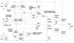
Did you put your output transistors TIP122 on heatsinks. If not you've blown them. It sounds from your diagnosis that you have blown at least one of them anyway.
These are Darlington transistors and are really not suitable for this type of circuit.
These are Darlington transistors and are really not suitable for this type of circuit.
As Bone says 🙂
Also the lower TIP122 should have a resistor B to E to help speed up transistor turn off. The bias arrangement of two diodes might work in simulation but real world and it can be a whole different ball game. I would add emitter resistors of at least 0.33 ohm to both TIP's and replace the two diodes with a vbe multiplier that is in contact with the heatsink.
Also the lower TIP122 should have a resistor B to E to help speed up transistor turn off. The bias arrangement of two diodes might work in simulation but real world and it can be a whole different ball game. I would add emitter resistors of at least 0.33 ohm to both TIP's and replace the two diodes with a vbe multiplier that is in contact with the heatsink.
Hi
There are a few minor things to look at, and one particular issue. First, the current mirror should have some emitter degeneration, ~100R or so. You need a DC blocking cap. A bi-polar electrolytic in series with Rfb2 to GND. Cdom is way to large, should be about 1/10th or less than what it is. You might try some leading compensation by placing a zero (small pf cap in series with a resistor) between the collector of Qvas to the base of Qdif-fb. You should include a 'turn off' resistor from collector of Qclassb- to V-. The output transistors need at least to have a resistor from base to emitter otherwise they will not turn off fast enough to prevent cross conduction. This may be part of why the output(s) failed. Now for the particular issue, the temperature coefficient of the output transistors is not matched by the bias diodes. There has to be some sort of thermal feedback from the outputs to the biasing components because as temp rises Vbe decreases and so having a static bias for the outputs will result in an increase in bias as temp rises resulting in destruction after a period of time of operation, look up thermal runaway. If the intent is pure class B, meaning some of the output waveform will be missing resulting in distortion, then thermal runaway is less of a problem. But the idea is for class AB where both output devices bias a small current. These output transistors are Darlington devices. Because both integrated transistors are on the same die, they are at the same temperature. The result of this is that the overall temperature coefficient is the product of the temp coefficient from both transistors that are inside the component. Compensating this with a single PN junction as with the diodes will not accomplish adequate thermal compensation. A+B does not equal AXB. You need to use a Vbe multiplier with a Darlington transistor as the thermal sensing device. Also you need to have some small emitter degeneration for the output transistors, like 0.3 Ohms or so. This will help in bias stability and better linearize the output transconductance significantly reducing distortion. This circuit looks like a text book example of an audio amplifier for basic understanding, but as usual the details that make it work are left out.
Evidently Mooly beat me to some of the points, guess I took too long to type😀
Last edited:
An input resistor to ground would help things in a practical build.
Without an input (and without an input resistor) this amplifier will latch up to the rail.
Without an input (and without an input resistor) this amplifier will latch up to the rail.
Hi, I'm an Electrical Engineering college student and I just finished designing and building my first amplifier. It's a 3 stage BJT amp, although of note is that we ran out of PNP power transistors so I had to use a quasi-complementary output stage. Anyway, my problem is that the simulation works perfectly (for my requirements) and I built the circuit on a bread board and then a perfboard and it worked (i.e. both a sine wave and music came out louder and without noticeable distortion). However, I must have blown something because now the output is just a DC offset and the amp maxes out the current from the negative power supply rail. Both the breadboard and the perfboard are having this problem, and I have been trying to troubleshoot them for a few weeks now as well as just flat out rebuild the circuit many times without any luck. I attached the circuit I am using.
I would really appreciate if you could give me any thoughts as to why I might be having this problem, any general trroubleshooting tips (this is my first time actually building an analog circuit - I'm relatively clueless), or if there is anything inherently wrong with my design.
Thank you,
Laptopdude
Previous messages have given you some info but not the big picture. This is a classical example of design by simulator, where you have included a fair amount of sophistication in the form of blocks you can do a 'copy-paste' with, but then fail to address some really simple issues - this fails because it shows you do not have enough basic understanding of the circuits in question, so you do not know how to 'ask' pf the simulation the required 'what-if' questions.
Remember, the simulation will only give you a fair aproximation OF THE SIMULATED CIRCUIT, and note capitals because a real circuit is NOT the simulated one.
Take the example of the missing resistor from input to ground. A simulation will never tell you that it's missing because the internal resistance of the source takes it's place - and if you look at the schematic, you can't see this drawn as a resistor, it's incorporated into the source symbol. But without it, the base current of the left input differential transistor cannot folow and therefore with no source attached the input differential cannot work. Now, if you knew this you would have simulated the circuit without the source attached and discovered something was wrong, and eventually what.
Then there is the case of the missing base resistor from the bottom TIP122 to minus rail. There IS a resisitor of sorts there, but again you have a problem because you cannot see it, neither the fact the TIP122 is a darlington, with 2 transistors, two resistors and a diode all inside the package. However, the connection of the resistors inside, even though it does provide some means of taking out the base charge and turning off the transistor(s) is woefully inadequate. You see, your simulation does not show that real transistors have input and reverse capacitances which need to be charged and discharged in time with the amplified signal. There ARE some capacitors in the model, but they are not shown in the symbol. And, if you knew that, you could have checked your simulation say at 20kHz or 50kHz and looked at some currents and found that things are not exactly simple.
Finally, the current mirror. This will work in a simulation just fine, because all transistors of the same type in a simulator behave EXACTLY the same, since they use exactly the same model. Real world transistors have tolerances as high as 400% on some parameters and others change as much depending on operating point. So, some circuits need a means to reduce the parameter spread, and a current mirror is one glaring example. In order to know how to use a simulator and how to interpret it's results, one needs to understand what it was made for and at least to a limited extent, how and what it does. Nearly all simulators are based on a SPICE simulator core program, which was initially developed to simulate the behavior of integrated circuits. This has consequences - the program assumes all parts are at the same temperature and all parts of a type have exactly the same characteristics, which is a fair assumption since all of them are made at the same time with the same tolerances on the same silicon die. To apply this to the real world requires knowledge of the real world - a simulation is NOT the real thing, one should never forget this.
Someone has mentioned the biasing arrangement with 2 diodes. This will under-bias the output stage because the drivers and outputs all in all have 4 B-E junctions in series. As one poster mentioned A+B does not equal AxB, in this case the bias voltage is way too low so thermal runaway should not be a problem. If you do not know what the term means, then you should not have tried to design the thing in the first place - because you will not understand why real world bias is not fixed - and then, you will also check in your simulator what it is at different temperatures (bet you didn't think of that) and found some interesting things to think about.
Also, how about checking what happens when the input signal is large enough the amp will attempt to drive the output beyond the voltage of the power rails? Check that at high frequency, say 20k? Tried that? All of this is quite normal for any amp, even the simplest one, and it should be able to reliably cope with that situation because in the real world power supplies do not come on instantly, inputs can appear before the power supplies do, when the source is connected there can be transients, etc.
Which brings me to the 5k resistor which is the load for your VAS. You have included a sophisticated current source in the tail of the input differential and augmented the gain of that stage by a current mirror - yet used the worst possible load for your VAS. Ask yoursef, would it be reasonable to conclude you have fully understood how the circuits work?
In other words you should be able to construct and analyse the circuit in broad terms on paper using a calculator. Checking if it works is NOT just putting an input signal at the input and checking if it comes out amplified - especially not in a simulator. A simulator will gladly simulate a 'working' circuit with transistors well outside their permissible ranges of operation whereas in the real world they will turn to smoke. And unless you know what to check in a simulator, the only result you will have in the real world is smoke, and no idea why - for that you have to know HOW IT WORKS. A simulator will not tell you this and you simply cannot learn it from a simulation, this would be like figuring out how a car engine works by driving the car. A simulator will only tell you 'how much' it works once you already know the how and why, so you can check points, voltages, currents, transient responses, frequency and phase responses, power dissipation etc in the simulator. It cannot interpret or check any of the for you.
- Status
- Not open for further replies.
- Home
- Amplifiers
- Solid State
- Troubleshooting a 3 Stage BJT Amp