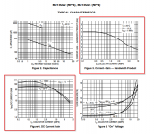
Hi I'm looking at this transistor datasheet MJ15024. I was looking for a Ic/Vce diagram for linearity but it does not provide it. But they do provide a current gain / Ic graph. Would it be correct to say that the linear part of the gain is the linear part of the transistor ?
Thx
Thx
Attachments
If the junction temperature is constant transistors are linear throughout their usable range.
The hfe varies with temperature and current flow. That is why a power transistor needs at least enough hfe to produce from the base current the required output.
Linearity is corrected with negative feedback in amplifiers.
The hfe varies with temperature and current flow. That is why a power transistor needs at least enough hfe to produce from the base current the required output.
Linearity is corrected with negative feedback in amplifiers.
I think it is clear from the data sheet graphs that this transistor is a lot of things, but not linear.
The question was: is the transistor linear range the same as the gain linear range. That's an ambiguous question, it depends on what is meant by 'transistor linear range'.
Jan
The question was: is the transistor linear range the same as the gain linear range. That's an ambiguous question, it depends on what is meant by 'transistor linear range'.
Jan
The source of the question is that this transistor and his PNP brother are used in class A with a suggested bias between 1.2A and 2A, works fine either way. I was just wondering.

The transistor BJT is a current amplifier. The collector current is equal to the product of the base current by Hfe (non-linearly dependent on the current). In the scheme with CC (EF) the transistor amplifies the current, but does not amplify the voltage.
Class A assumes the operation of the transistor without switching. In this sense, the mode of operation is linear with a certain assumption.
Last edited:
In one sense BJTs are highly non-linear, having an exponential dependence of load current on Vbe, and Vbe is what drives carrier injection from emitter into the base which is the actual physical mechanism of the device.
However the base current also has an exponential dependence on Vbe, so it can be thought of as roughly linear as a current amplifier, but the current gain is not very stable, and most uses of BJTs use a circuit topology that linearizes the gain with local feedback. Current gain varies a lot between devices so such circuit topologies are used also to mitigate variations between devices.
For output devices the beta v. current graphs provide a useful guide to the open-loop "large signal" distortion properties of the device, and yes there typically is a region of constant beta until the current gets large (all BJTs have this, but good output devices delay the onset of this gain "droop" considerably - for instance compare the poor performance of the old 2N3055 with the more modern 2SC3281).
The MJ15024 you mention also shows a nice flat part of the gain graph. Note that in a class B amplifier the matching of gain between NPN and PNP devices is also important for gain linearity, reducing any gain discontinuity at the cross-over point.
Last edited:
The transistor BJT is a current amplifier. The collector current is equal to the product of the base current by Hfe (non-linearly dependent on the current). In the scheme with CC (EF) the transistor amplifies the current, but does not amplify the voltage.
Class A assumes the operation of the transistor without switching. In this sense, the mode of operation is linear with a certain assumption.
That's the right curve 😉
In class A, you place the bias point in the middle of the curve where the curve is almost a line. If you have a signal level not to high, you stay in a portion of the curve where it stays a line. If amplitude increases then you go to part of the curve which is no more a line -> distortion of signal increases. This is why Class A is the best class for high-fidelity and this is why the efficiency is so poor (Power with no signal is VxI at bias point and is not null. In a class A-B your are in the portion of the curve where either the voltage is near 0 or either the current is near 0 so Power is near 0).
- Home
- Amplifiers
- Solid State
- Transistor linear region equal to linear gain region ?