I am working on a hiraga 30w amp, it has an iddle at 1.65 amps and produces alot of heat, I was not happy about die temperature versus heatsink temperature.
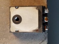
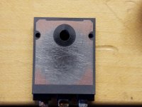
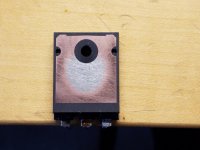
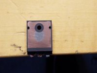
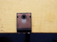
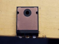
I bought a very fine coarse wetstone for sharpening knives, its surface seems extremely smooth almost like porcelain, I started polishing one output device as shown, you can see that it removed more on the outer surface like it has a deepening in the centre where the die is mounted, it took 15 minutes to get the entire surface even, heat transfer has improved by some degrees actually.
Anybody else tried this approach?
Attachments
Yes, I've also used grinding paste and T-cut before now and 10mm thick glass as a flat surface. There's a lot of info here ESP - Heatsink design and transistor mounting
I would also suggest using Belleville washers
I would also suggest using Belleville washers
Hi.
Great to hear I was in doubt if my finding was an error, a complete smooth even surface must be ideal to transfer heat, I can also feel it if I place it on a mirror, it sticks, most be due to smoother surface, the devices I left alone didn't have that effect.
Great to hear I was in doubt if my finding was an error, a complete smooth even surface must be ideal to transfer heat, I can also feel it if I place it on a mirror, it sticks, most be due to smoother surface, the devices I left alone didn't have that effect.
That's a good sign, air gaps are the issue.I can also feel it if I place it on a mirror, it sticks, most be due to smoother surface, the devices I left alone didn't have that effect.
Yes, both surfaces must be perfectly flat.
Some transistor datasheets actually state acceptable or guaranteed flatness in the mechanical drawings section.
Some transistor datasheets actually state acceptable or guaranteed flatness in the mechanical drawings section.
Yes I have used this method in the past and whenever I can, it helped the transfer of heat tremendously on this project here,
how can test the stator insulation and mylar coating?
Cheers !!
jer 🙂
how can test the stator insulation and mylar coating?
Cheers !!
jer 🙂

I'd love to see measurement data before vs after with good statistical significance. Otherwise, unless the application is direct metal-to-metal between the device and the heatsink, the performance of thermal interface material always dominates, therefore, the flatness of a device usually does not matter. The pressure from the torque/tension of the fasteners can cause a warpage you can never buff out anyways. If concerned, stop using fasteners through the device's mounting hole, and use spring clips of known, consistent hold-down pressure instead.
By the way, I can't stop suspecting that the particular transistor you took to a sharpening stone had a mounting surface carefully engineered to have a slightly higher surface around the perimeter than in the center where the hole is, so that when a correct tightening torque is applied, the interfacing surfaces would be flattened out perfectly by the fastener's tension.
By the way, I can't stop suspecting that the particular transistor you took to a sharpening stone had a mounting surface carefully engineered to have a slightly higher surface around the perimeter than in the center where the hole is, so that when a correct tightening torque is applied, the interfacing surfaces would be flattened out perfectly by the fastener's tension.
Large copper directly to transistor, and a mica sheet underneath fastened with spring clamp or actual springs, for continuous pressure ragardless of temperature.
I learned a great deal today, and very helpful now that I reached a mature age and have taken great interest in class a designs
I learned a great deal today, and very helpful now that I reached a mature age and have taken great interest in class a designs
Has anyone measured a temperature difference between lapped and unlapped transistors and heat transfer? Does it make an audible difference?
Just wondering if this is really necessary. Of course, it's your time and effort. Does it make a 10 degree C difference?
Just wondering if this is really necessary. Of course, it's your time and effort. Does it make a 10 degree C difference?
I use silpads so the gaps are filled by the pad.
Best silpad is no silpad.
I once built an amp in a wooden enclosure and used two heatsinks, one for pnp and the other for npn and no silpads. Open backed box and it worked a treat.
Best silpad is no silpad.
I once built an amp in a wooden enclosure and used two heatsinks, one for pnp and the other for npn and no silpads. Open backed box and it worked a treat.
When finances allow I will invest in some temperature dataloggers,
The cheapest Chinese multimeter and thermocouple 🙂
I just use an infra red thermometer, point and shoot the laser.
Absolutely invaluable.
You can also see difference between temp of transistor and heat sink.
Absolutely invaluable.
You can also see difference between temp of transistor and heat sink.
I reworked a local guys SS guitar amp awhile ago...I had to reposition the board & the power transformer. It was originally in a metal case & likely was well organized inside, whoever modded it did a lousy job. The single TDA-2050 had a scrap piece of aluminum as a heat-sink. I redid the sink with what I had on-hand...since I was winging it & the device was "freestanding", I reasoned I could attach pieces of aluminum on both sides of the device...of course the "traditional" side, but the other side, the smaller tab of the device, above the plastic as well. This addition looked roughly like the wings of a dragonfly, slightly bent so that the air-space between the traditional sink & the "front" new sink, isn't so close to each other.
Just trying to think out-of-the-box.
-----------------------------------------------------------------------Rick.......
Just trying to think out-of-the-box.
-----------------------------------------------------------------------Rick.......
A good observation and good solution.I bought a very fine coarse wetstone for sharpening knives, its surface seems extremely smooth almost like porcelain, I started polishing one output device as shown, you can see that it removed more on the outer surface like it has a deepening in the centre where the die is mounted, it took 15 minutes to get the entire surface even, heat transfer has improved by some degrees actually.
Anybody else tried this approach?
The copper base is stamped in a group in line, that is called a leadframe. 10, 20 in a row, designed for automatic die attach and wirebonding.
The stamping is what causes the concavity of the surface, because the last punch operation was top to bottom.
Lapping as you did will certainly help heat transfer. Otherwise, the thicker paste in the center will not transfer much heat flux, it has to spread horizontally away from the die.
If you lap it nice and flat, and use a really thin amount of paste, that will be good.
If you really want to get the best, use an intermediate copper plate at least 50 mils thick, also lapped both sides, and use a thin graphene sheet to the plate, and use isolation under that. You spread out the heat transfer more efficiently that way.
The whole idea is to widen the area of transfer so that the heat flux density is much lower by the time it gets to the paste. Paste and mica are poor thermal transfer materials. Graphene sheet is supposedly better than copper, but electrically conductive.
I recently autopsied several power supplies, TO-254's where the edge of the case did not have the overmolded plastic, and the copper edge cut through the insulator. For those, I used 2000 grit as it used sheets of silpad heat transfer material that was 5 mils thick.
Jn
Last edited:
- Home
- Amplifiers
- Solid State
- Transistor heat transfer capability