Hi,
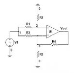
Please give me the transfer function of the following circuit. Where R1,R2,R3,R4 and R5 are not equal.
You should check out a neat little program called sapwin 😉
Just remember that the voltages at inverting and noninverting inputs are equal, that the current flowing into the inverting and noninverting inputs is zero, and it will be pretty easy to set up the basic equations to solve for Vo/Vi.
it actually "safer" to explicitly include op amp gain "A" and derive the equations
you can always take the limit as A goes to infinity later - but by assuming it from the start you may save a term or two in the calculations or you may have your solution "blow up" from the infinity you are implicitly carrying around
the op amp Howland current source is a favorite nasty problem set for those not understanding the "null injection" implicit infinity
@DF96
I am not a student in any institute so do not expect any Marks.
@SY, jcx
Thank you, I solved it using superposition theory.
R1 and R2 forms voltage divider for Non-Inv voltage. R3||RD forms Rg and R4 forms Rf. So Non-Inv, Inv output voltage will be
Vninv = V1*[R2/(R1+R2)]*[1+{R4/(R3||RD)}]
Vinv = V1*-(R4/R3)
Vout = Vninv + Vinv
Good. Sorry for jumping to conclusions, but your question looked like homework.sameerdhiman said:I am not a student in any institute so do not expect any Marks.
I'm not certain that your result is correct. I would expect to see two simultaneous equations involving Vin and Vout, which you then invert to get Vout in terms of Vin. What is RD?
Sorry, R5=RD (In practical circuit R5 will be variable resistor e.g. JFET or LDR)
I've verified the equation with LTSpice.
If you any other equation/solution please post that.
I've verified the equation with LTSpice.
If you any other equation/solution please post that.
OK, I see how you have done it. Split node 1 into two independent inputs, then add the result. What confused me was your nomenclature: I assumed that Vninv was the voltage at the noninverting input, when in fact it is the output due to the input at the noninverting input.
Now you got it. 🙂
Vninv is non-inverting output voltage which is equal to
Vinput * Resistor-Divider Output * Non-Inverting Gain
Vinv is inverting output voltage which is equal to
Vinput * Inverting Gain
Final output voltage will be sum of Vninv and Vinv
Am I correct ?
Vninv is non-inverting output voltage which is equal to
Vinput * Resistor-Divider Output * Non-Inverting Gain
Vinv is inverting output voltage which is equal to
Vinput * Inverting Gain
Final output voltage will be sum of Vninv and Vinv
Am I correct ?
I fell into the same tiger trap as DF96.
Vinv = input voltage at -IN pin.
Vninv = input voltage at +IN pin
Silly me for reading what it said,
Instead I should have reverse engineered the given equations and realised that Voutinv=Vinv and Voutninv=Vninv are the only way to make your equations work correctly !!!!
Vinv = input voltage at -IN pin.
Vninv = input voltage at +IN pin
Silly me for reading what it said,
Instead I should have reverse engineered the given equations and realised that Voutinv=Vinv and Voutninv=Vninv are the only way to make your equations work correctly !!!!
- Status
- Not open for further replies.
- Home
- General Interest
- Everything Else
- Transfer Funtion of the given circuit ?