Hi everyone!
I am building a amp with 3x TPA3255 amplifiers, 3x PCM5242 DACs, 2x PCM1802 ADCs, 1x ADAU1466 DSP, and also a PCM2706 USB to I2S converter. I already got a rough board layout + schematic sketched up but would like some help on some questions I still have.
First of all, grounding is my biggest concern. As of now I have a continuous ground place on both sides of my 2 layer PCB. Everything shares the same ground plane, and I use partitioning to keep digital signals away from the sensitive analog ones, in addition to using separate analog and digital regulators. However, since one of my aims is low noise from the amplifier, I heard if the analog ground plane is not kept separate, the high current switching of the class D amplifiers will manifest as noise on the outputs? Should I use a separate analog plane or keep it as a continuous ground plane?
Secondly, I am also contemplating splitting the amplifiers into different modules. There are 3 amplifier blocks (each with a TPA3255 IC configured in BTL mode) with resistors to set the master/slave configuration for switching synchronization, and 1 DSP/signal processor board that handles the 12V supplies, Power on/off reset control, in addition to the ADCs, DACs, etc. However, if I go this path, I am even more concerned with grounding, since there are multiple boards with ground now. My main concern is ground loops, which I had tons of issues with previously and had to go with isolated dc-dc converters, which I am avoiding in this design. So how should I design my board in this case? Should I have a AGND lead connecting to the AGND of the TPA3255 IC, which connects to the AGND of the signal processor board, like a star ground? The grounds will still be connected to the main ground, but do I really need to keep the analog reference ground separate?
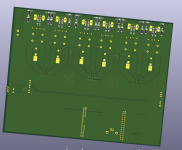
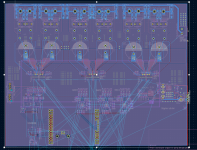
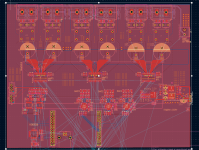
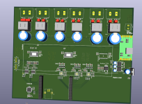
Attached below are my unfinished layout and schematic. I haven't completely finished this design because I am really struggling in grounding and help will be greatly appreciated!
(One thing I want to mention is that the PCM5242 IC outputs a differential signal to the power amp ICs, but don't amplifiers still have limited noise rejection even in a differential signal? And wouldn't the return current spikes affect the sensitive ADCs used for the analog inputs?)
I am building a amp with 3x TPA3255 amplifiers, 3x PCM5242 DACs, 2x PCM1802 ADCs, 1x ADAU1466 DSP, and also a PCM2706 USB to I2S converter. I already got a rough board layout + schematic sketched up but would like some help on some questions I still have.
First of all, grounding is my biggest concern. As of now I have a continuous ground place on both sides of my 2 layer PCB. Everything shares the same ground plane, and I use partitioning to keep digital signals away from the sensitive analog ones, in addition to using separate analog and digital regulators. However, since one of my aims is low noise from the amplifier, I heard if the analog ground plane is not kept separate, the high current switching of the class D amplifiers will manifest as noise on the outputs? Should I use a separate analog plane or keep it as a continuous ground plane?
Secondly, I am also contemplating splitting the amplifiers into different modules. There are 3 amplifier blocks (each with a TPA3255 IC configured in BTL mode) with resistors to set the master/slave configuration for switching synchronization, and 1 DSP/signal processor board that handles the 12V supplies, Power on/off reset control, in addition to the ADCs, DACs, etc. However, if I go this path, I am even more concerned with grounding, since there are multiple boards with ground now. My main concern is ground loops, which I had tons of issues with previously and had to go with isolated dc-dc converters, which I am avoiding in this design. So how should I design my board in this case? Should I have a AGND lead connecting to the AGND of the TPA3255 IC, which connects to the AGND of the signal processor board, like a star ground? The grounds will still be connected to the main ground, but do I really need to keep the analog reference ground separate?
Attached below are my unfinished layout and schematic. I haven't completely finished this design because I am really struggling in grounding and help will be greatly appreciated!
(One thing I want to mention is that the PCM5242 IC outputs a differential signal to the power amp ICs, but don't amplifiers still have limited noise rejection even in a differential signal? And wouldn't the return current spikes affect the sensitive ADCs used for the analog inputs?)
Attachments
Update:
After doing further readings, it seems that it does not seem necessary to separate grounds for the PCM5242s and the TPA3255s. According to TIDA-00874 (High Fidelity 175-W Class-D Audio Amplifier with Digital Inputs and Processing Reference Design), the PCM5242s are connected to the same ground as the TPA3251 (less powerful version of the TPA3255), which is why I used a ground plane in the design. The idea is further supported in TIDA-01414 (TPA3244 Dolby Atmos Soundbar Reference Design), which uses multiple TPA3245 amps and PCM5252 (PCM5242 with more DSP capabilities, such as smartbass), but uses one ground plane for everything. So it seems like the general consensus for the DACs is that I am going to be using a common groundplane with good return paths for the powerstage, and also maybe use a 4 layer pcb (2oz each for all 4 layers).
However, a large question still remains. While the output stage (DAC + amp) is solved, I still have questions about the input stage (ADC part). Since I am using a PCM1802 for the input, the input itself is single ended and I believe that it is prone to picking up the switching noise of the amp from the ground plane. So in this case what grounding approach should I use? Should I create a separate AGND island for just the ADCs which forms a star ground with the ground plane at some point? Should I use opamps that feed into a ADC that uses differential inputs? Should I use a whole different ADC ic like the PCM1863? I would like some advice here since I am lost in this area.