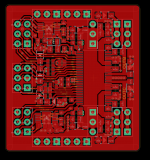
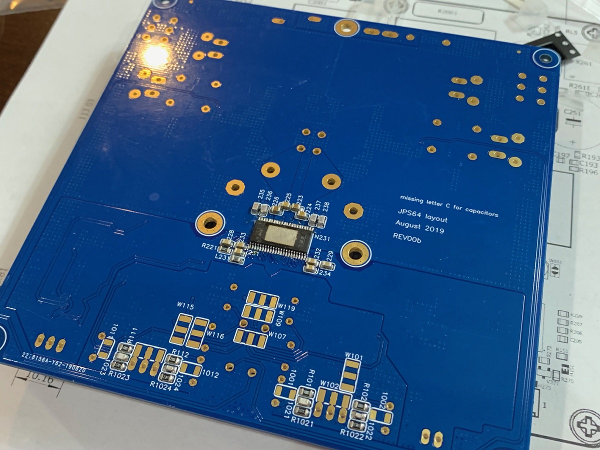
Have been fiddling around with TPA3255 pcb-s for few weeks and i got idea to make some sort of "interposer" pcb that will house basic small smd parts, aux voltage regulators and protection diodes.
still need to find way to manufacture some form of heat spreader that will shield whole pcb and be soldered on ends, also think soldering it to chip would be better than thermal compound.
chip working modes can be selected external to this "core pcb" and other pcb could easlily be made one sided and all with tht components for easy assembly.
what do you people think about this approach for simplifying diy with TPA3255 chips for universal use with different kinds of end solutions?
thanks on info
Attachments
I see a single-sided pcb, no PVDD bulk caps, no output inductors. This may or may not work - somehow - but definitely not in the ballpark of the TI ref design.
not sure you read it, or even looked at attached picture for that matter. it is not single sided pcb, see those vias. it is dual sided with ground plane on bottom layer its just omitted from picture to better see whats going on on pcb, pvdd bulk caps like rest of tht components and inductors are meant to be on big pcb, so it is not full and it cant work without main pcb. since term "core". also so i can use same "core" pcb for 4channel, 2.1, 2.0 and mono amplifiers as needed just changing big pcb with tht components and different cooling solutions preferably s775 cpu cooler or similar for easy assembly at home and still have end pcb that is small.
Last edited:
Sorry, but I can not see any vias on your pcb. I understand your motivation of a minimal module, but the constraints due to longer wires at sensitive points will degrade performance. And with the picture of the top with its restricted resolution it is hard to judge the layout.
All in all it depends on your personal design goals😉
All in all it depends on your personal design goals😉
Looks like a nice tight neat layout. I kind of get Voltwides concerns in respect of power and output filtering but conceptually as something that is going to drop down onto a main board there does not seem to be too much, if any, compromise in terms of routing to, should be easier, or routing lengths to, those components. You kind of get a four layer board for free plus chunky tracks.
If you were to place the power passives on the same board I really cannot see how things would work out to be any tighter both physically and logically.
I like it. Very DIY given most people playing with these ICs are buying pre-built modules and messing about with power filtering capacitors and output filter configurations. The base board should logically follow on and would be much easier for someone to lay out for themselves then drop yours on top.
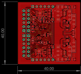
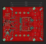
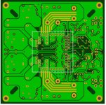
thank you on feedback, here is bit updated layout with more pvdd connections and thicker power traces, also in higher resolution. dimensions is 4x4cm, it is not yet final layout.
added freq and overcurrent control on outside pins that you can short to gnd if using stock setting.
tomorrow will make "main" pcb and try to do some form of 3d to try to visualise better.
i think main pcb could be made single sided with little effort but need to check.
added freq and overcurrent control on outside pins that you can short to gnd if using stock setting.
tomorrow will make "main" pcb and try to do some form of 3d to try to visualise better.
i think main pcb could be made single sided with little effort but need to check.
Attachments
voltwide , you have not seen this RDC2-0034a, Усилитель мощности класса D. TPA3255, PurePath, 315Вт Stereo или 600Вт Mono | купить в розницу и оптом
Now that I have seen it, this is a quite different approach with a more complete "kernel", i.e. PVDD blocking Elcos etc...voltwide , you have not seen this RDC2-0034a, Усилитель мощности класса D. TPA3255, PurePath, 315Вт Stereo или 600Вт Mono | купить в розницу и оптом
Btw, I would not consider a single-sided pcb for the main board, and there is no cost advantage nowadays in doing so.
Very sexy in a meant to be way. I guess the big headache would be the cooler and how it is, mechanical sandwich, mounted to your Core/Base. It does kind of shout a standard CPU lever type attachment on the main board but you might need something a bit custom in terms of the lump of heat sink metal for proper interfacing . Just dreaming.
@drMordor interesting pcb but local PVDD decoupling caps are bit far from chip pins for my liking.
@MorbidFractal it should be easy to put some thermal compound and solder shield around but i would like to solder machined copper not only on edges of board but also on chip itself. still not sure is that worth effort tho. should fit in socketed cpu cooler height, mount bulk caps and inductors on bottom and should be nice small amplifier.
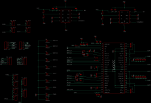
here in attach schematics of this core 4x4 pcb..
@MorbidFractal it should be easy to put some thermal compound and solder shield around but i would like to solder machined copper not only on edges of board but also on chip itself. still not sure is that worth effort tho. should fit in socketed cpu cooler height, mount bulk caps and inductors on bottom and should be nice small amplifier.
here in attach schematics of this core 4x4 pcb..
Attachments
Last edited:
It’s an interesting idea. But the large through hole components are the easy part. What is gained from putting them on a separate “motherboard”, and thereby making the distance farther away? The low impedance paths from the TPA to the inductors, filters, and input Vdd and bulk caps is critical. They are not going to be optimal of placed on separate board - for what advantage does this provide?
I have used the motherboard and core amp module daughterboard concepts before. For example, the Yarra preamp motherboard - which then allows different preamp topology modules to be installed and swapped. Here, there is no need to swap - the core is the only amp.
I mount the TPA3255 on the bottom side so that thermal pad can be clamped to mounting surface as heatsink (with a thermal spreader):
It then simplifies top side for mounting all the required ancillary parts:
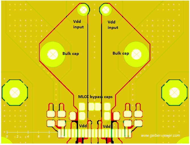
To highlight what an example of placing the Vdd input and bulk caps as close to TPA3255 pins as possible could look like:
I have used the motherboard and core amp module daughterboard concepts before. For example, the Yarra preamp motherboard - which then allows different preamp topology modules to be installed and swapped. Here, there is no need to swap - the core is the only amp.
I mount the TPA3255 on the bottom side so that thermal pad can be clamped to mounting surface as heatsink (with a thermal spreader):
It then simplifies top side for mounting all the required ancillary parts:
To highlight what an example of placing the Vdd input and bulk caps as close to TPA3255 pins as possible could look like:
Last edited:
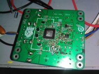
thanks on info, please attach pictures so no confusion, have used similar layout with chip on pcb bottom on my tas5630b prototype pcb, see attached picture 1,2.
also have TPA3255 prototypes in work and ordered that also use same layout see pic 3.
this should be beneficial for people who dont want to bother with smd soldering, but still want good if not very good performance from said chip. simple as that.
you could also mount bulk caps beneath with similar distance from chip pins but still have place for lets say post filter feedback components and all tht no need to solder smd, also idea is to have some form of heat spreader that is soldered directly on chip so using pc cpu cooler would be simple with cheap thermal compound.
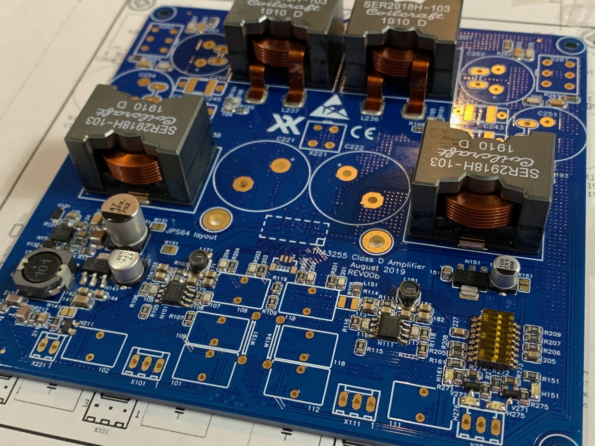
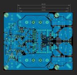
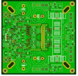
on picture 4,5 is stereo pcb 10*8cm in early works but i think it could be nice... not sure about bulk caps distance i think around 3.5cm. will check tomorrrow.
also have TPA3255 prototypes in work and ordered that also use same layout see pic 3.
this should be beneficial for people who dont want to bother with smd soldering, but still want good if not very good performance from said chip. simple as that.
you could also mount bulk caps beneath with similar distance from chip pins but still have place for lets say post filter feedback components and all tht no need to solder smd, also idea is to have some form of heat spreader that is soldered directly on chip so using pc cpu cooler would be simple with cheap thermal compound.
on picture 4,5 is stereo pcb 10*8cm in early works but i think it could be nice... not sure about bulk caps distance i think around 3.5cm. will check tomorrrow.
Attachments


Last edited:
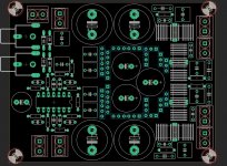
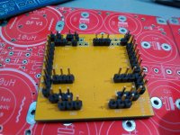
small update, main pcb for stereo amp finished, core module mounts on bottom, 10x8cm ,should fit 72,78,85mm intel coolers, post filter feedback, all tht, have good feeling about this pcb, after some checking up will order pcbs and will update here how it works if at all.
Attachments
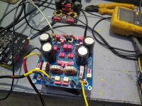
diy soundcard for basic tests, will give away few finished boards to someone here who have better test equipment and are wiling to post results, if thing will work reliably that is.
only issue is i sold my scope as i am moving soon so i am bit blind.
still need to add fan control to pcb, and small thermistor on core pcb.
only issue is i sold my scope as i am moving soon so i am bit blind.
still need to add fan control to pcb, and small thermistor on core pcb.
main and core pcb prototypes ordered, now only thing left is where i can machine copper heatspreder for cheap, and wait for parts to arrive.
slot holes are made to accept intel lga775, lga1156, lga1366 coolers with some nuts and washers for start or screw directly into casing/shielding of whole pcb if i manage to manufacture it somehow.
10x10cm pcb.
will update here but it take time. have fun.
slot holes are made to accept intel lga775, lga1156, lga1366 coolers with some nuts and washers for start or screw directly into casing/shielding of whole pcb if i manage to manufacture it somehow.
10x10cm pcb.
will update here but it take time. have fun.
Attachments
Last edited:
pcbs should arive at 3-4 weeks from now sry i dont have pcb fabrication available localy or even parts.
![IMG_20191201_204311[1].jpg](/community/data/attachments/727/727487-7603ed67336898207f192de2953ad429.jpg?hash=dgPtZzNomC)
![IMG_20191201_204322[1].jpg](/community/data/attachments/727/727500-ae8a6ef86a4ee8d342adeb7eac532d30.jpg?hash=ropu-GpO6N)
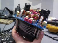
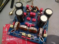
finaly managed to finish up.
well finish prototype, on todo list still some stuff:
add fan smps + pwm temperature controller
refine both main and core pcb, goal not make it larger than 10x10/2layers but tht
find way to cheaply manufacture heatspreder
find way to connect core pcb without soldering, for easy replacement/diy
now i used cheap thermal pad on core pcb, any kind soul with good measuring equipment and spare time and will want to measure this thing? will send it for free.
Attachments
-
 IMG_20200117_132341.jpg738.8 KB · Views: 157
 -
 IMG_20200117_132352.jpg795.7 KB · Views: 112
 -
 IMG_20200117_145732.jpg874.4 KB · Views: 148
 -
 IMG_20200117_204116.jpg575.5 KB · Views: 140
 -
 IMG_20200117_150517.jpg971.3 KB · Views: 142
 -
 IMG_20200117_204414.jpg902 KB · Views: 135
 -
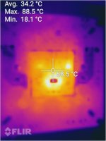 flir_20200117T201545.jpg268.6 KB · Views: 114
 -
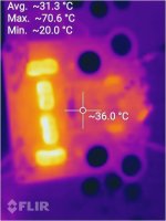 flir_20200117T205822.jpg258.2 KB · Views: 107
- Home
- Amplifiers
- Class D
- TPA3255 Core PCB