I dedicate audio 40 years, I never disclose their topology until the last years. Here is one of my latest amplifier topology.
An externally hosted image should be here but it was not working when we last tested it.
Site photos
An externally hosted image should be here but it was not working when we last tested it.
Technical parameters of PS
Size 108 x 170 mm
Strength 2.5 and 3 mm
Strength Cu 75 and 105μm
Double-sided, plated
Solder mask, printing, tin plating
Technical parameters of amplifiers 4Ω
Driver HQQF-55-502D
Involvement HQQF-55-503W-4-2
End transistors 2 x 4 x IRFP240/9240
Power supply AC 230V + 2 x 48V (I recommend 300 ÷ 800W)
Cooler, thermal resistance of 0.20 ÷ 0.08 ° C / W, according to the transformer
Rectifier bridge 35 (25) A non-PS
Filtration 16 x 1m/100V (16mF ÷ 64mF)
Additional filtering capabilities block 48 x 1m/100V, separate PS
Worm Up Maximum output voltage ± 65V (46V UEF)
Burden, typically 4Ω
Power, maximum 2 x 500W (2 x 250W/8Ω)
Current protection around 17A
BOM components 4Ω!
Amplifier is to dimension the continuous maximum power transformer using 1.5 kW, which is required to use the cooler thermal resistance of 0.04 ° C / W (not recommended)
Technical parameters of amplifiers 2Ω
Driver HQQF-55-502D
Involvement HQQF-55-503W-4-2
End transistors 2 x 4 x IRFP240/9240
Power supply AC 230V + 2 x 34V (I recommend 300 ÷ 800W)
Cooler, thermal resistance of 0.20 ÷ 0.08 ° C / W, according to the transformer
Rectifier bridge 50 (35) A non-PS
Filtration 16 x 2m2/63V (35mF ÷ 140mF)
Additional filtering capabilities block 48 x 2m2/63V, separate PS
Worm Up Maximum output voltage ± 45V (32V UEF)
Burden typical 2Ω
Power, maximum 2 x 500W (2 x 250W/4Ω, 2 x 125W/8Ω)
Current protection around 35A
BOM components 2Ω!
Amplifier is to dimension the continuous maximum power transformer using 1.5 kW, which is required to use the cooler thermal resistance of 0.04 ° C / W (not recommended)
Technical parameters of amplifiers 8Ω
Driver HQQF-55-502D
Involvement HQQF-55-503W-4-2
End transistors 2 x 4 x IRFP240/9240
Power supply AC 230V + 2 x 66V (I recommend 300 ÷ 800W)
Cooler, thermal resistance of 0.20 ÷ 0.08 ° C / W, according to the transformer
Rectifier bridge 25 (35) A non-PS
Filtration 16 x 1m/100V (16mF ÷ 64mF)
Additional filtering capabilities block 48 x 1m/100V, separate PS
Worm Up Maximum output voltage ± 92V (65V UEF)
Burden typical 8Ω
Power, maximum 2 x 500W
Current protection around 8.5 A
BOM components 8Ω!
Amplifier is to dimension the continuous maximum power transformer using 1.5 kW, which is required to use the cooler thermal resistance of 0.04 ° C / W (not recommended)
I always look at the amplifier's own eyes. I described the causes Transistor sound here.
Federmann Bohumil. Tranzistorový zvuk počítačové simulace příčin jeho vzniku. Perspektivy elektroniky v roce 2009: 26. 3. 2009. Rožnov pod Radhoštěm: SŠIEŘ RPR, 2009, s. 19-25. ISBN 978-80-254-4052-0.
Please add your experiences.
Federmann Bohumil. Tranzistorový zvuk počítačové simulace příčin jeho vzniku. Perspektivy elektroniky v roce 2009: 26. 3. 2009. Rožnov pod Radhoštěm: SŠIEŘ RPR, 2009, s. 19-25. ISBN 978-80-254-4052-0.
Please add your experiences.
i notice there are emitter followers to drive all those output mosfets. therefore, i'm curious about the distortion versus frequency performance.
Milloyd,
Where are the emitter followers you mention? I can't see any EFs ANYWHERE in his circuit in Post #1.
Regards, Allen (Vacuum State)
Where are the emitter followers you mention? I can't see any EFs ANYWHERE in his circuit in Post #1.
Regards, Allen (Vacuum State)
therefore, i'm curious about the distortion versus frequency performance.
I would like to see measured distortion plots vs. frequency and amplitude as well, into 4 ohm.
sorry, you're right allen. i meant to say "I notice there are NO emitter followers to drive all those output mosfets"
i notice there are emitter followers to drive all those output mosfets. therefore, i'm curious about the distortion versus frequency performance.
I dedicate audio 40 years, I never disclose their topology until the last years. Here is one of my latest amplifier topology.
An externally hosted image should be here but it was not working when we last tested it.
after a quick inspection, I noticed the following:
1) only N-channel MOSFETs: I think, in the negative half you must use P-channel devices by the presently used driver topology
But better solution it must be, to use only N-Channel MOSFETs (to get more information, go to my link collection about
http://www.diyaudio.com/forums/soli...better-audio-non-complements-audio-power.html
2) the average connection of the potentiometer for the idle current to the base to the transistor for the variable voltage source isn't a good solution, because the max possible idle current (shorting current of your power supply) runs through the output devices in case of a pot-break. Replace your potentiometer between base and emitter and introduce a fixed resistor between collector and base to this transistor. This must be done always, not only in this case.
But the input circuit looks very interesting
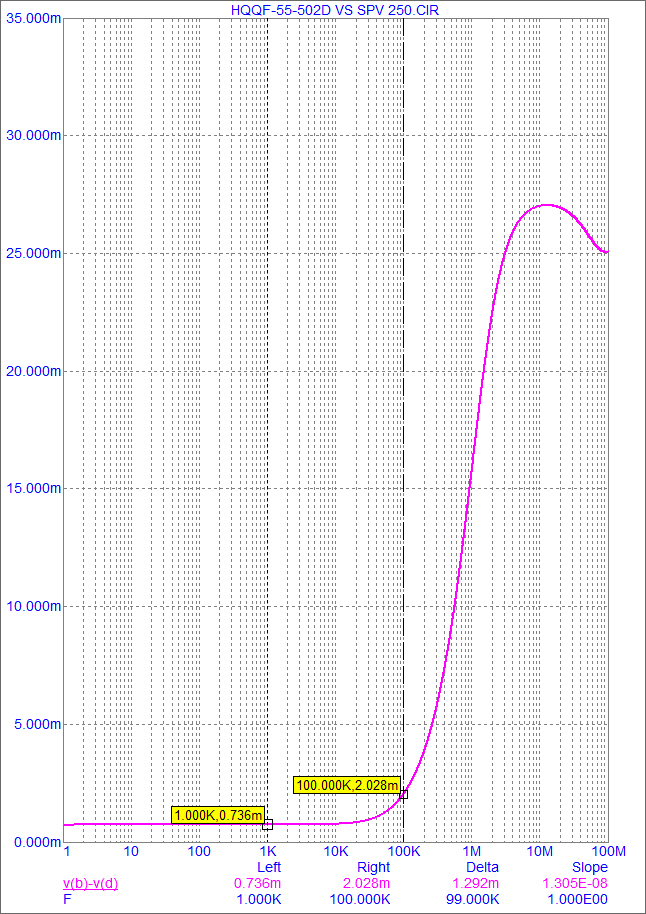
Characteristics of my drivers HQQF-55-502D, amplification without feedback. I set up to focus on flat transmission characteristics. Warning phase characteristics of the different scale
An externally hosted image should be here but it was not working when we last tested it.
But the input circuit looks very interesting
The input circuit is pretty conventional isn’t it?
What about gate stoppers?
Cheers
Characteristics of drivers HQQF-55-502D feedback and intensifying 26dB, is worth noting a very small phase angle in the acoustic band, watch a different phase characteristic scale
An externally hosted image should be here but it was not working when we last tested it.
The input circuit is pretty conventional isn’t it?
What about gate stoppers?
Cheers
you are right. the kind of schematic drawing got me confused - it is a mirror symmetric differential amp for high open loop gain, that is find in some amps.
Input circuit drivers HQQF-55-502D is in no way exceptional, but the currents are unusually large, the result is:
• Increased gain
• Flat Specifications
• Small Udif (differential voltage input)
Stages Ufif
• Increased gain
• Flat Specifications
• Small Udif (differential voltage input)
Stages Ufif
I know that we shall see no distortion measurements. Only a sort of nothing saying simulations. Maybe a photo of a finished amp, and oscilloscope screenshots as well??
PMA is certainly right, but the simulations SPICE_kompatibile usually very not different.
Preparation for construction.
Preparation for construction.
Last edited:
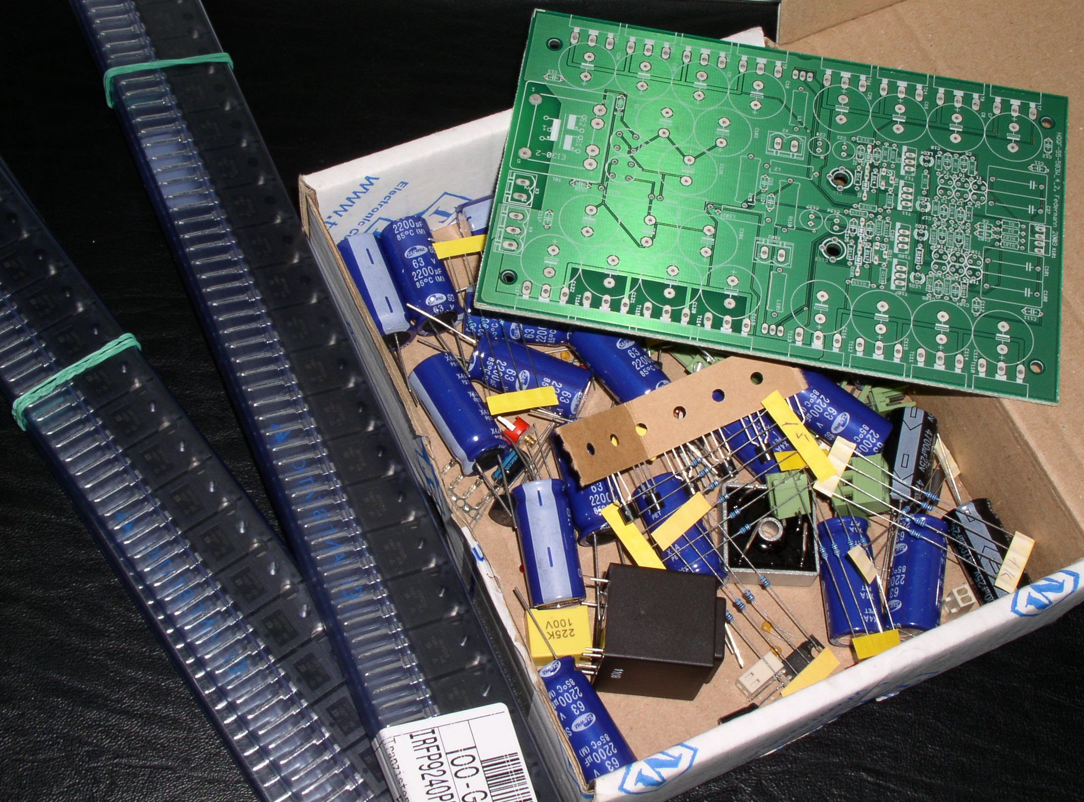
Current form, the assessment and fitting end transistors. He will be measured.
An externally hosted image should be here but it was not working when we last tested it.
Oh, I see...at this point your PCB make fuse effect, trace is correctly wide - very clever... 🙂
Not wash yet ? And what are these disgusting spots on the left side ? Perspiratory relicts of intensive soldering ? 🙂
Not wash yet ? And what are these disgusting spots on the left side ? Perspiratory relicts of intensive soldering ? 🙂
I am not talking about lines commonly, but only about one - between Boucherot devices...there I see only c. 0,3 mm, which is little bit thick...but maybe after some drinks I will see something different like you... 🙂
- Status
- Not open for further replies.
- Home
- Amplifiers
- Solid State
- Topology Federmann, HQQF-55 ...