I'm currently trying to build a digital guitar pedal, and right now I just want to be able to hear the signal being amplified correctly. I'm going for 44.1kHz at 256Fs.
Gear being used:


5V comes out of the USB connection from the STM32 with my laptop, from a 5V pin in the dev board. The STM32 is outputting a clock of 256Fs = 11.2896MHz as SCLK for the ADC & DAC. The ADC is set as I2S master, and it outputs the I2S audio clock (BCLK) for the DAC.


The problem is that the ADC output is too noisy and distorted. Sounds like heavy static with a little bit of guitar coming through, distorted. I thought it was the DAC, but the logic analyzer readings confirm it (output from a E note on the 12th string, with 6x gain):


The gain stage output seems to be fine (don't mind the readings, it's DC coupled but I switched to AC coupled on the scope):

I'm thinking it's because of my setup, as I'm prototyping everything in solderless breadboards, and the long wires and all the intertwining is transforming it into a big antenna (maybe?):

So far I've tried:
Do you guys have any idea why this is happening? Will it go away if I etch a board or use a perforated board?
Gear being used:
- STM32H743VIT6 as MCU (on a dev board)
- PCM1808 as ADC (on a module)
- PCM5102A as DAC (on a module)
- OPA2376 and MCP6022 input & output 5V rail-to-rail op amps
- the DAC output is being fed to my USB audio interface
5V comes out of the USB connection from the STM32 with my laptop, from a 5V pin in the dev board. The STM32 is outputting a clock of 256Fs = 11.2896MHz as SCLK for the ADC & DAC. The ADC is set as I2S master, and it outputs the I2S audio clock (BCLK) for the DAC.
The problem is that the ADC output is too noisy and distorted. Sounds like heavy static with a little bit of guitar coming through, distorted. I thought it was the DAC, but the logic analyzer readings confirm it (output from a E note on the 12th string, with 6x gain):
The gain stage output seems to be fine (don't mind the readings, it's DC coupled but I switched to AC coupled on the scope):
I'm thinking it's because of my setup, as I'm prototyping everything in solderless breadboards, and the long wires and all the intertwining is transforming it into a big antenna (maybe?):
So far I've tried:
- inserting an 1k resistor inbetween the DAC_OUTPUT and the output buffer.
- decreasing the input gain and using unity gain
Do you guys have any idea why this is happening? Will it go away if I etch a board or use a perforated board?
Last edited:
Possibly..I'm thinking it's because of my setup, as I'm prototyping everything in solderless breadboards, and the long wires and all ..
Will it go away if I etch a board or use a perforated board?
My first assumption would be too much gain, if unity gain did not stop the issue.
Maybe clock settings or clock signal.
Or looking at the buffer shown in the post, it is single supply there will half supply dc offset on the output.
Ill assume there is ac coupling capacitor somewhere not shown with load resistor to ground
Maybe clock settings or clock signal.
Or looking at the buffer shown in the post, it is single supply there will half supply dc offset on the output.
Ill assume there is ac coupling capacitor somewhere not shown with load resistor to ground
Last edited:
If I remember correctly a guitar can leave a few volts top voltage when you hit all strings hard and have max volume out on the guitar.
It is easy to check with an oscilloscope. I believe your input amplifier might clip even with a zero gain.
You can reduce that a bit if you change the C21-R27 link to a higher cutoff frequency. The E string is 82Hz so you will have no problem with a 30 Hz crossover.
It is easy to check with an oscilloscope. I believe your input amplifier might clip even with a zero gain.
You can reduce that a bit if you change the C21-R27 link to a higher cutoff frequency. The E string is 82Hz so you will have no problem with a 30 Hz crossover.
I think clock configuration may be a problem.
First, SPI receiving only 11 MHz that may be too low, counting few internal clock dividers in the SPI itself.
Secondly, HSI (RC based) may be too jittery for I2S use. Try with HSE crystal or HSE bypass mode driven by external low noise clock.
I'd run uCPU at max 480, and SPI close to DS limits, 120 or so
Huh? Being master means you generate the clocks. So if the STM32 is generating the I2S clocks it should be the master. I2S devices require stable clocks, quartz-derived (with low jitter) is a requirement.The STM32 is outputting a clock of 256Fs = 11.2896MHz as SCLK for the ADC & DAC. The ADC is set as I2S master,
I have another worry with the setup. You have a gain of about 6, are you sure a guitar never outputs transients above 400mV peak?
Thanks for the replies, guys!
One more thing I noticed only now is that: I'm running the guitar signal into the ADC's left channel, and out of the DAC's "LROUT" output. I don't know what that means, some sort of mono output? Anyway, nothing comes out of the left channel from my audio interface:

But with the right channel I can hear the output:

The ADC module decouples the signal as the ADC datasheet recommends and it has a 2.5V VREF point internally, so even though the amplified signal is centered around 2.5V, it's coming out decoupled as the ADC plots show. That's why I haven't tried putting an AC coupling cap before, but I tried it now and no success - still a lot of noise and distortion.
I'll try unity gain again and I'll try switching C21 and R27 values, thanks!
I don't know much about sampling theory, but why is 11.2896MHz not enough? How can I calculate how much the SPI itself eats off the clock frequency?
I also think clock config is a culprit, because the circuit is only working (= I'm being able to hear it) when the STM32 outputs clock from the HSI at 11.2896MHz. Outputting ~11.2896MHz from the HSE isn't working somehow.
The ADC datasheet states that it can operate as master by receiving the appropriate sampling frequency clock. In that case the STM32 outputs this clock (SCLK), and then the ADC internally generates the audio/bit clock (BCLK) and WS/channel clock (LRCK), which will drive both the STM32 and the DAC.
I also tried setting the STM32 as master but somehow it didn't output the clock, my logic analyzer got literally nothing. Could be wrong connections, I will post an update on this approach later.
One more thing I noticed only now is that: I'm running the guitar signal into the ADC's left channel, and out of the DAC's "LROUT" output. I don't know what that means, some sort of mono output? Anyway, nothing comes out of the left channel from my audio interface:
But with the right channel I can hear the output:
My first assumption would be too much gain, if unity gain did not stop the issue.
Maybe clock settings or clock signal.
Or looking at the buffer shown in the post, it is single supply there will half supply dc offset on the output.
Ill assume there is ac coupling capacitor somewhere not shown with load resistor to ground
The ADC module decouples the signal as the ADC datasheet recommends and it has a 2.5V VREF point internally, so even though the amplified signal is centered around 2.5V, it's coming out decoupled as the ADC plots show. That's why I haven't tried putting an AC coupling cap before, but I tried it now and no success - still a lot of noise and distortion.
If I remember correctly a guitar can leave a few volts top voltage when you hit all strings hard and have max volume out on the guitar.
It is easy to check with an oscilloscope. I believe your input amplifier might clip even with a zero gain.
You can reduce that a bit if you change the C21-R27 link to a higher cutoff frequency. The E string is 82Hz so you will have no problem with a 30 Hz crossover.
I'll try unity gain again and I'll try switching C21 and R27 values, thanks!
I think clock configuration may be a problem.
First, SPI receiving only 11 MHz that may be too low, counting few internal clock dividers in the SPI itself.
Secondly, HSI (RC based) may be too jittery for I2S use. Try with HSE crystal or HSE bypass mode driven by external low noise clock.
I'd run uCPU at max 480, and SPI close to DS limits, 120 or so
I don't know much about sampling theory, but why is 11.2896MHz not enough? How can I calculate how much the SPI itself eats off the clock frequency?
I also think clock config is a culprit, because the circuit is only working (= I'm being able to hear it) when the STM32 outputs clock from the HSI at 11.2896MHz. Outputting ~11.2896MHz from the HSE isn't working somehow.
Huh? Being master means you generate the clocks. So if the STM32 is generating the I2S clocks it should be the master. I2S devices require stable clocks, quartz-derived (with low jitter) is a requirement.
I have another worry with the setup. You have a gain of about 6, are you sure a guitar never outputs transients above 400mV peak?
The ADC datasheet states that it can operate as master by receiving the appropriate sampling frequency clock. In that case the STM32 outputs this clock (SCLK), and then the ADC internally generates the audio/bit clock (BCLK) and WS/channel clock (LRCK), which will drive both the STM32 and the DAC.
I also tried setting the STM32 as master but somehow it didn't output the clock, my logic analyzer got literally nothing. Could be wrong connections, I will post an update on this approach later.

My understanding, that you don't use SPI at all, just supply MCLK to ADC, and feed I2S stream from ADC directly to DAC?
Anyway, I know for sure that HSI clock is a crap, so better to find another one.
Okay, the ADC can operate as I2S clock master, but in that case its incoming MCLK signal (master clock) needs to be from a very low jitter crystal clock, or if you want cheap maybe from an MEMS clock. Those clocks should be on clean power too; not dirty MCU power if you want tolerably low jitter.The ADC datasheet states that it can operate as master by receiving the appropriate sampling frequency clock.
Maybe it would help to explain this way: Every ADC and every DAC needs two low noise analog references. There is an analog time reference (clock) and an analog voltage reference. So why is a clock an analog reference? Its because what matters is not high or low like would matter for a digital logic signal. Rather, what does matter is the exact timing between the clock edges. Variation in that timing is referred to as jitter in the time domain, or as phase noise in the frequency domain. OTOH, voltage reference noise is in the form or amplitude variation. So, you may read about AN versus PN noise effects in data converters. Bottom line that MCUs are poison as far as low noise analog clock sources. Bad as low noise analog voltage references too (such as PWM-based). Even the power rail noise generated by MCUs is a real problem.
Last edited:
View attachment 1448898
My understanding, that you don't use SPI at all, just supply MCLK to ADC, and feed I2S stream from ADC directly to DAC?
Anyway, I know for sure that HSI clock is a crap, so better to find another one.
Yes, for now I'm only using the STM32 to provide the clock, ADC and DAC are connected directly.
I'll fiddle with the clock settings to discover why I can't output clock using HSE (I just hope the dev board one isn't failing)
Okay, the ADC can operate as I2S clock master, but in that case its incoming MCLK signal (master clock) needs to be from a very low jitter crystal clock, or if you want cheap maybe from an MEMS clock. Those clocks should be on clean power too; not dirty MCU power if you want tolerably low jitter.
Maybe it would help to explain this way: Every ADC and every DAC needs two low noise analog references. There is an analog time reference (clock) and an analog voltage reference. So why is a clock an analog reference? Its because what matters is not high or low like would matter for a digital logic signal. Rather, what does matter is the exact timing between the clock edges. Variation in that timing is referred to as jitter in the time domain, or as phase noise in the frequency domain. OTOH, voltage reference noise is in the form or amplitude variation. So, you may read about AN versus PN noise effects in data converters. Bottom line that MCUs are poison as far as low noise analog clock sources. Bad as low noise analog voltage references too (such as PWM-based). Even the power rail noise generated by MCUs is a real problem.
The HSE crystal on the dev board is a YXC 25MHz, do you think it's clean enough? I'll try to get it working. So you guys recommend have the STM32 as master, using HSE?
Thanks for the clarification on the noise types. In my case, I'm experiencing both?
Probably.In my case, I'm experiencing both?
Also, there are two families of standard audio clock frequencies. Lower frequency clocks tend to produce lower levels of phase noise. Higher frequency clocks allow for high sample rates.
For most DSP purposes, one clock family is chosen, most commonly the 48kHz family. Some standard clock frequencies for the 44.1kHz family are: 11.2896MHz, 22.5792MHz, and 45.1584MHz. For the 48kHz family some standard frequencies are: 12.288MHz, 24.576MHz, and 49.1520MHz. These values from the table at: https://en.wikipedia.org/wiki/Crystal_oscillator_frequencies
In order to run on one clock frequency only, many DSP chips have ASRC (asynchronous sample rate converter) functions available for incoming digital audio.
Last edited:

Which device should be I2S master depends on what clocks the ADC and the DAC chip use for actual conversion of digital to analog. The ADC may use MCLK, the dac may use MCLK or maybe LRCK. Since LRCK is an I2S clock, it should be very low jitter if that's what the dac is using for conversion. If you want to use the MCU do act as I2S bus master, I would consider reclocking and galvanic isolation before going into the dac. I have a thread on that if any interest in looking through it: https://www.diyaudio.com/community/threads/general-purpose-dac-clock-board.413001/ There is also a simplified board available in the thread at: https://www.diyaudio.com/community/...2soverusb-pcm2dsd-rtz-dac.423401/post-7917601 It also includes provision for hosting I2SoverUSB.
That said, the problem with some of this stuff is, although it can help lead to very good sound, unfortunately its not super low-cost like most guitar effects are. Of course, that's why some digital guitar effects sound so bad.
The other thing about guitar effects is that things like fuzz pedal effects produce harmonic distortion which can cause digital aliasing. For such reasons its not uncommon for nonlinear guitar effects to be upsampled to much higher sample rates before effect processing. Then they can be anti-alias filtered and decimated down to the output data converter (DAC) sample rate. Something like that.
Last edited:
Before delving into clocks how have you configured the ADC (MD1, MD2, FMT pins)? MD0 & MD1 should be high (256fs) and FMT low (I2S). Also you should change the "Data24 Bit Alignment" setting of MCU to "Data 24 Bit Alignment Left".The HSE crystal on the dev board is a YXC 25MHz, do you think it's clean enough?
To use HSE crystal you first have to enable it in RCC configuration.The HSE crystal on the dev board is a YXC 25MHz, do you think it's clean enough? I'll try to get it working.
Attached is what I would use as clock configuration with 25MHz HSE and MCO2.
Attachments
With the ADC as master I was doing:Before delving into clocks how have you configured the ADC (MD1, MD2, FMT pins)? MD0 & MD1 should be high (256fs) and FMT low (I2S). Also you should change the "Data24 Bit Alignment" setting of MCU to "Data 24 Bit Alignment Left".
MD1 & MD0 <= 3.3V
FMT <= GND
I changed the alignment to "Left" but it seemed to have no impact. Also, why is the alignment "left" when the I2S standard puts a 1 bit left-padding, shifting the data bits to the right? Shouldn't it be "alignment right"? I get the functionality, but this naming is weird.
Thanks, I tried your clock setup but still, this was the ADC output with 2x gain on the opamp:
~2x gain, 44.1kHz, ADC as master

~2x gain, 44.1kHz, ADC as master

~2x gain, 44.1kHz, ADC as master
~2x gain, 44.1kHz, ADC as master
~2x gain, 44.1kHz, ADC as master
I also tried 48kHz, with STM32 as master:
ADC:
MD1 & MD0 <= GND
FMT <= GND
~2x gain, 48kHz, STM32 as master

~2x gain, 48kHz, STM32 as master

~2x gain, 48kHz, STM32 as master
~2x gain, 48kHz, STM32 as master
~2x gain, 48kHz, STM32 as master
The fact that this "dislocated noise" only happens on the negative of the sine wave should tell something, but I still don't understand.
Which device should be I2S master depends on what clocks the ADC and the DAC chip use for actual conversion of digital to analog. The ADC may use MCLK, the dac may use MCLK or maybe LRCK. Since LRCK is an I2S clock, it should be very low jitter if that's what the dac is using for conversion. If you want to use the MCU do act as I2S bus master, I would consider reclocking and galvanic isolation before going into the dac. I have a thread on that if any interest in looking through it: https://www.diyaudio.com/community/threads/general-purpose-dac-clock-board.413001/ There is also a simplified board available in the thread at: https://www.diyaudio.com/community/...2soverusb-pcm2dsd-rtz-dac.423401/post-7917601 It also includes provision for hosting I2SoverUSB.
That said, the problem with some of this stuff is, although it can help lead to very good sound, unfortunately its not super low-cost like most guitar effects are. Of course, that's why some digital guitar effects sound so bad.
The other thing about guitar effects is that things like fuzz pedal effects produce harmonic distortion which can cause digital aliasing. For such reasons its not uncommon for nonlinear guitar effects to be upsampled to much higher sample rates before effect processing. Then they can be anti-alias filtered and decimated down to the output data converter (DAC) sample rate. Something like that.
Thanks for the explanation. I have a PCM3060 CODEC here, do you think I'll get better results using it in a PCB?
See reference manual figure 638:Also, why is the alignment "left" when the I2S standard puts a 1 bit left-padding, shifting the data bits to the right? Shouldn't it be "alignment right"? I get the functionality, but this naming is weird.
So your configuration is the 3rd row. With right alignment the frame is padded with zeros from left. Your ADC sends left aligned data (see figure 24 in PCM1808 datasheet).
You should see a clear difference between right and left alignment.
Have you looked at the I2S signals coming from ADC with a scope?
Oh thanks, now I get it.So your configuration is the 3rd row. With right alignment the frame is padded with zeros from left. Your ADC sends left aligned data (see figure 24 in PCM1808 datasheet).
Have you looked at the I2S signals coming from ADC with a scope?
You mean the clocks?
LRCK:
BCK:
Checks out, right?
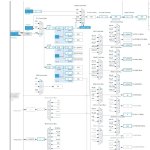
Can you draw a diagram that shows how you feed the clocks to your DAC in both cases (ADC as master / STM32 as master). Also how have you configured your DAC?I also tried 48kHz, with STM32 as master
So STM32 is currently only used for generating the clocks?
Can you draw a diagram that shows how you feed the clocks to your DAC in both cases (ADC as master / STM32 as master).
(I removed the output buffer between the DAC output and the output jack)
The connection stays the same for both cases, only difference is that when the ADC is the master, I2S1_MCK comes from a different pin (an MCO pin, MCO2 = PC9). When STM32 is the master, I2S1_MCK comes from PC4:
Yes, I thought it would be easier to check if the signal is being properly read by the ADC & DAC first.So STM32 is currently only used for generating the clocks?
Last edited:
If STM32 is only generating clocks I would just use ADC master mode. You can still use I2S MCK clock from PC4. If it still does not work I don't think it is related to MCK as clock generated from HSE should be good enough.
- Home
- Design & Build
- Electronic Design
- Too much noise and distortion out of ADC fed with guitar signal