As usual, I had some screwball ideas bout how to improve an amp (Apex's
version of some Elector thing?) that got all way out of hand and off topic.
So much so, I decide early, on my own, to spare this poor soul my thread-
jacking delusional rant. And just start up this new delusional rant instead.
Anyways, the subject up for debate: Exactly what Class is it?
I'll open the debate by suggesting that it crosses like a Visch. But note
that additional constant current always flows, so nothing ever actually
tuns off... Though 1A idle current here seems very hard to justify as a
Visch Class crossing? Its obviously not Visch B. Yet both transistors do
sorta shut down, but only to a very high impedance CCS like state...
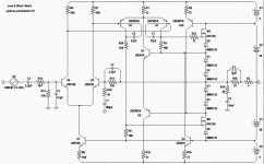
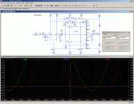
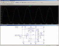
My crossing is illustrated at 22KHz into 4ohms, and just shy of clipping.
Idle currents pivot on tricking Schottky Diodes to operate on the curve.
I don't try to predict or force an exact quiescent. Only depend it will be
usefully more than zero, and usefully less than what would otherwise bias
a cold Schottky to its nominal voltage drop. Thats what Visch does, true???
You see NO resistors in this output totem, yet I suspect it is completely
thermally stable, especially if the bipolar comparators are allowed to share
in the output temperature, but the Schottkys are kept far away.
I can't really classify this as B, A, Hyperbolic A, nor even a true AB.
Is one allowed to call it AB even though nothing ever "B" shuts off?
HyperAB, VischAB, what exactly do we got here???
These transistors are only the closest available LTSpice default models.
Not necessarily representing ideal choices for Safe Operating Area.
version of some Elector thing?) that got all way out of hand and off topic.
So much so, I decide early, on my own, to spare this poor soul my thread-
jacking delusional rant. And just start up this new delusional rant instead.
Anyways, the subject up for debate: Exactly what Class is it?
I'll open the debate by suggesting that it crosses like a Visch. But note
that additional constant current always flows, so nothing ever actually
tuns off... Though 1A idle current here seems very hard to justify as a
Visch Class crossing? Its obviously not Visch B. Yet both transistors do
sorta shut down, but only to a very high impedance CCS like state...
My crossing is illustrated at 22KHz into 4ohms, and just shy of clipping.
Idle currents pivot on tricking Schottky Diodes to operate on the curve.
I don't try to predict or force an exact quiescent. Only depend it will be
usefully more than zero, and usefully less than what would otherwise bias
a cold Schottky to its nominal voltage drop. Thats what Visch does, true???
You see NO resistors in this output totem, yet I suspect it is completely
thermally stable, especially if the bipolar comparators are allowed to share
in the output temperature, but the Schottkys are kept far away.
I can't really classify this as B, A, Hyperbolic A, nor even a true AB.
Is one allowed to call it AB even though nothing ever "B" shuts off?
HyperAB, VischAB, what exactly do we got here???
These transistors are only the closest available LTSpice default models.
Not necessarily representing ideal choices for Safe Operating Area.
Attachments

Last edited:
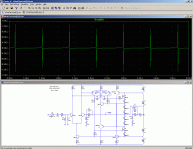
Let me revise this to say that Schottky diodes D1-D4 can and do turn off.
But no transistors in this scheme ever do. And even though MOSFETs do
not have a tail current to worry if they were to shut off, they can store
a big excess pull-down charge on the gates. Keeping them hovering just
above threshold of shut-down proves as beneficial as it does for BJTs.
I've also found that I can ditch Q4 and Q10 and just span 100R across the
D1-D4 string to set a minimum current to flow in both output devices at
all times. And of course, Schottkys D1-4 also keep the load from stealing
away any of that minimum current.
Feeding a small portion of Q9's collector current into R8 also helps auto-
set a good working bias. But too much of this feedback starts oscillation.
But you could series about 10K atop 180R and feed Q9C into the smaller
resistor. After that mod is done, you no longer need Q7 or the -59 rail.
One less 9V regulated cord wart to hide! Now if I can figure how to get
rid the top 9V Wart? But small wart sims so much better than bootstrap,
and easily drives the output to within 2V of the +50 power rail.
Yeah, I know, no more CCS anywhere after Q7 is stripped out! But then
again: You got Q9 and Q3 as shunt regulators, constantly shunting away
any excess bias. Actually seems to work. I need to draw you the Muntz
minimal version as described, but time is short today. Maybe tomorrow.
Last edited:
I don't think your circuit qualifies as a "Visch", but it is nevertheless very interesting.
In my opinion, the core of the Visch concept is to store in a cap the average reference voltage used to create and control the quiescent current.
Your circuit is different, the control is purely static. Which, in my opinion is a good thing, but much more difficult to achieve without creating oddities in the crossover region.
I note that you have a somewhat schizophrenic approach of your own circuit: on one hand, you create an elaborate circuit with diodes and current sources to insure a minimal current always flows in the output devices, and on the other hand, you completely destroy this functionnality by forcing the MOSFETs to run at a much larger current.
Basically, with your current values the operation is as follows: Q3 and Q9 require M1 M2 to pass a high enough current in the diode string D1 to D4, so that their voltage drop is sufficient to keep them on the verge of conduction.
The rest of the circuit is pretty irrelevant, and this can be demonstrated by disabling the current sources Q4 Q10, and shorting out D5 D6: there is practically no difference.
The circuit can be made to operate in the way originally intended by that other part of your mind:
D2 and D3 are changed to silicon diodes, and the control circuit becomes free to operate: the transition is now much sharper, with a lower current, but no transistor ever shuts down: it becomes a non-switching class B.
But in this case, I think the usual problems associated with this kind of circuit will appear: a kwirky transfer function in the crossover region.
Attachments
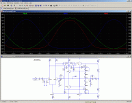
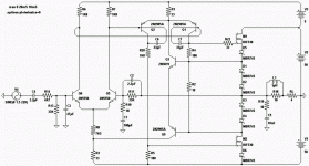
The circuit can be made to operate in the way originally intended by that other part of your mind: D2 and D3 are changed to silicon diodes
Those diodes are key components that must shut down and recover quietly.
(indeed they are the only parts that ever shut down) Therefore they have to
be Schottky. With junction diodes, there is going to be tail currents that will
result in the power devices trying to shut off instead. Schottky also happens
to have the square law curve going for it.
I do compare Schottky voltage curves against silicon junction emitter drops.
But my BJT emitter drops are biased well above the worst of their curve, and
never asked to elegantly handle a shutdown. Wasn't that the whole point???
Last edited:
The rest of the circuit is pretty irrelevant, and this can be demonstrated by disabling the current sources Q4 Q10, and shorting out D5 D6: there is practically no difference.
I agree the current sources can be ditched, but not their functionality.
A simple bleed resistor across the fixed voltage span does the trick in
my second spin of this circuit (Post# 6 & 7).
As for D5 D6, they replaced 0.1R source degeneration resistor that seemed
helpful at higher frequency. However 0.1R dropped too much voltage with
large signals. Copy and paste Schottky from the output bridge in place of
the 0.1R. Seemed to do the trick quite nicely. Check at 22K or above and
look for signs of a small trailing edge ring without D5 D6.
D5 and D6 are not in the part of the circuit that shuts down. You will see
the difference the constant current makes if you measure there (or at the
MOSFETs) instead of at the output bridge diodes.
Last edited:
Those diodes are key components that must shut down and recover quietly.
(indeed they are the only parts that ever shut down) Therefore they have to
be Schottky. With junction diodes, there is going to be tail currents that will
result in the power devices trying to shut off instead. Schottky also happens
to have the square law curve going for it.
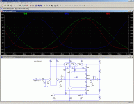
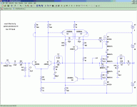
OK then, just add one more schottky to the string:
Attachments
- Status
- Not open for further replies.
- Home
- Amplifiers
- Solid State
- To Visch or not to Visch?