Some of us like to use various output stage Included compensation networks for their amplifiers design.
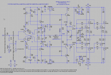
To use Tian or Middlebrook prob, in order to look at the Loop gain, we need to cut the line that goes from output to the feedback bridge (that fix the closed loop gain).
Once this connection is broken, and replaced by the prob, I wonder where is better to set the compensation signal source. Before the prob (power output stage side) or after (feedback bridge) ?
(See attached)
Attachments


Good question indeed.
I remember somewhere in definitions of Middlebrook/Tian approaches was written that there must not exist closed NFB loops not detached by the probe.
Your first example is just an example for this. So I bet for the second variant (and actually all of simulation of your schematic I did was this way).
I remember somewhere in definitions of Middlebrook/Tian approaches was written that there must not exist closed NFB loops not detached by the probe.
Your first example is just an example for this. So I bet for the second variant (and actually all of simulation of your schematic I did was this way).
Attachments
Thanks for your care, arpagon. (Is your pseudo a reference to Molière ? ;-)Good question indeed.
I remember somewhere in definitions of Middlebrook/Tian approaches was written that there must not exist closed NFB loops not detached by the probe.
Your first example is just an example for this. So I bet for the second variant (and actually all of simulation of your schematic I did was this way).
I agree on the definition. But, in my mind it advocates for the first example, no ?
In the second one, there is a closed local loop between output and VAS input with the compensation cap. But, with a traditional miller cap as well, in the VAS alone.
Hi Tryphoon,
Yes, the nickname is a wink to Moliere (but I'm not thrifty at all 😀).
Well, it was late when I answered you last night and I didn't realise that frequency compensation networks are not NFB loops in fact.
However, since changing the connection point of frequency compensation networks from input to the output of Tian's probe will directly alter the frequency compensation, I think they must stay where they are - directly attached to the amplifier's output.
Hi Tryphoon,
(but I'm not thrifty at all 😀).[/QUOTE]
I'm sure of this: you've already spent the "H" at the top of his name ;-)
Just like a miller cap between the collector and the base of the VAS transistors.
Thank-you for your help..
(but I'm not thrifty at all 😀).[/QUOTE]
I'm sure of this: you've already spent the "H" at the top of his name ;-)
I will follow your argument. It looks logical as it creates an unique block VAS+Output stage with all its poles and zeros (optimized by the compensation).Well, it was late when I answered you last night and I didn't realise that frequency compensation networks are not NFB loops in fact.
However, since changing the connection point of frequency compensation networks from input to the output of Tian's probe will directly alter the frequency compensation, I think they must stay where they are - directly attached to the amplifier's output.
Just like a miller cap between the collector and the base of the VAS transistors.
Thank-you for your help..

Very nice (Even harmonics) and low enough to not be an issue. And I tend to believe more in real measurements numbers than simulations ;-)You're welcome!
Keep us updated with your CFA. I also have a CFA but with modest numbers compared to yours 🙂. Here's a real measurement 100W/8 Ohm/1 kHz.
Fet based input stage, like your headphone amp ?
Very nice (Even harmonics) and low enough to not be an issue. And I tend to believe more in real measurements numbers than simulations ;-)
Fet based input stage, like your headphone amp ?
Ha, I hadn't believed someone here still remember this schematic. No, I replaced the FETs with Bipolars. This went to a little bit more complicated schematic but BC550/560 are cheaper by the dozen 😀.
Such replacement has a drawback though - in order to have only one stage with voltage gain, the input stage must work with currents equal to the currents of VAS. While it's normal when using FETs, it's not OK when using Bipolars due to the increased noise. In order to mitigate this I put a JFET Buffer in front of the input stage which eliminates the problem. The buffer's JFETs are cascoded the same way are cascoded the input transistors.
Well, quiet complicated on words 🙂.
- Status
- Not open for further replies.
- Home
- Design & Build
- Software Tools
- Tian prob question