MBoxler and DPH, thanks for both of your responses, although they seem to conflict with each other. If the unit is shipped with the solder bridges, which I think it is (I'll verify when I get home and can see it), I'm wondering why TI ships them with the solder bridges yet all other jumper defaults are for BTL (2 channel) operation. If DC was present on the outputs, I think my speakers would be toast by now, which they are working fine.
Actually, we are both right. If you have a DMM, and with no input signal, measure the voltage between OUTA and OUTB. This should measure ZERO volts. Now, measure the voltage between OUTA and ground. It should measure 1/2 of your supply voltage (24 volts if your supply is 48 volts). The voltage between OUTB and ground should also be 1/2 your supply voltage.
The fact that, with no input signal, there is +24 volts on your speaker + and +24 volts on your speaker - is no different than zero volts on both sides...the voltage potential between + and - is still zero.
As music plays, OUTA voltage is varying from +0 volts to +48 volts (max), while at the same time OUTB voltage is varying from +48 volts to +0 volts (max).
If OUTA is configured SE, than the signal must pass thru a capacitor to remove the 24 volt DC offset. Now you connect OUTA to speaker +, and ground to speaker -. Now, as music plays, OUTA voltage is varying from -24 volts to +24 volts (max), while at the same time ground is always at zero volts.
Does that help?
Mike
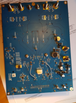
DPH please photo other side PCB.
Sorry, I guess I can get a photo, but the top side really just has the jumpers, connections, output inductors/coupling caps and a heatsink covering the chip. All the interesting bits are underneath, to be honest. Plus, the EVM manuals have a rendered view as well.
Mike -- we're 100% in agreement. Thanks for spelling it out better.
Dominique ,
very interesting idea - thx for bringing this up. The caps do indeed look like ceramic caps - and I am pretty sure that those can be improved upon - soundwise.
May I ask a question though:
I would like to do as you have done, i.e. bypass the input stage - I had similar good experiences when replacing input caps with transformers on a 3116 board. Anyway, I admit I am too stupid at the moment to figure out how you wired your RCA inputs - could you please explain (slowly - if you know what I mean -lol). Thx in advance.
I have the TI 3255 board btw.
Last edited:
Dominique was clever enough to take advantage of input headers that are just before the final caps. These headers aren't on the TPA3255EVM. However, it looks like one could use pins 11, 13, 15, and 17 of the AIB on the TPA3255EVM. Maybe???
Also appears that zero volts (RCA ground) goes to input B and input D. Therefore OUTA varies from zero volts to PS voltage, while OUTB sits at 1/2 PS voltage. Is that right Dominique?
Mike
Also appears that zero volts (RCA ground) goes to input B and input D. Therefore OUTA varies from zero volts to PS voltage, while OUTB sits at 1/2 PS voltage. Is that right Dominique?
Mike
Last edited:
I want to be 100% abundantly clear here, as what you quote back to me is not what I attempted to convey, and don't want people to get the wrong idea entirely and damage their equipment. As a note, this is all clearly spelled out in the EVM manual. I fully appreciate that we're getting a lot of folk coming through with varying electronics experience, but want to remind y'all the EVM manual is excellent. <snip>
Hi DPH,
Thank you for the explanation.I run my TPA3255 EVM SE input and have now removed the jumpers as per your excellent post.
Not needed if you're running the input single ended, but in bridged output. It's confusing, no? 🙂 Not really going to hurt anything though, but I apologize for further muddying the waters. As far as I know, the EVM manual is correct with all the jumper configurations relative to how the schematic is routed, so use that as a first reference.
Those soldered in jumpers are necessary for single ended output (which necessitates SE input, but I digress). You can have SE input, with bridged output (how the board is stock configured), where the input is buffered by the first inverting NE5532, then sent to the second NE5532 where it's inverted again. Now you have two copies being sent to Channels (A+B or C+D, respectively) that are in opposite phase.
Those soldered in jumpers are necessary for single ended output (which necessitates SE input, but I digress). You can have SE input, with bridged output (how the board is stock configured), where the input is buffered by the first inverting NE5532, then sent to the second NE5532 where it's inverted again. Now you have two copies being sent to Channels (A+B or C+D, respectively) that are in opposite phase.
Please note that the "not normal" way I currently test this very good amp board (feeding only one differential input,grounding second input per channel) has to my understanding at least the drawback of loosing amp power, and may be some other I have not encountered yet. I have heard an english sentence : who dares wins. I do not need currently a lot of power, but wants the upmost musical experience. A good amp should sound very good at low volume also and this one does. Therefore this test I take the risk for me -only-
Please have a look here TI doc : http://www.ti.com/lit/an/slaa719/slaa719.pdf
and for ex. page 2 see schematic "Cost Effective Input Stage" and text above. To avoid the dotted area I profit some the onboard headers. Mike has given the answer below for TPA3255. Please read the TPA3255 schematic for header usage.
Yes, was not aware of this difference between the two boards. Pins of AIB probably be used same way. Audio ground 1 (AGND1 in schematic) goes indeed to input B and AGND2 to input D. Have not measured yet the outputs, we can indeed expect what you wrote. Oh, I just saw another difference : on tpa3251 schematic, left/right grounds are marked different AGND1 and AGND2. On tpa3255 schematic there is only one label GND. Is there a signification difference on the boards, ground split,... leading to different behavior ? Please be aware of this.
So BOM in tpa3255evm documentation has an error. 10µF is also given by TI calculation spreadsheet. http://www.ti.com/lit/zip/slac733
I will try when I have 2 good caps of that value in hand.
Dominique ,
very interesting idea - thx for bringing this up. The caps do indeed look like ceramic caps - and I am pretty sure that those can be improved upon - soundwise.
May I ask a question though:
I would like to do as you have done, i.e. bypass the input stage - I had similar good experiences when replacing input caps with transformers on a 3116 board. Anyway, I admit I am too stupid at the moment to figure out how you wired your RCA inputs - could you please explain (slowly - if you know what I mean -lol). Thx in advance.
I have the TI 3255 board btw.
Please have a look here TI doc : http://www.ti.com/lit/an/slaa719/slaa719.pdf
and for ex. page 2 see schematic "Cost Effective Input Stage" and text above. To avoid the dotted area I profit some the onboard headers. Mike has given the answer below for TPA3255. Please read the TPA3255 schematic for header usage.
Dominique was clever enough to take advantage of input headers that are just before the final caps. These headers aren't on the TPA3255EVM. However, it looks like one could use pins 11, 13, 15, and 17 of the AIB on the TPA3255EVM. Maybe???
Also appears that zero volts (RCA ground) goes to input B and input D. Therefore OUTA varies from zero volts to PS voltage, while OUTB sits at 1/2 PS voltage. Is that right Dominique?
Mike
Yes, was not aware of this difference between the two boards. Pins of AIB probably be used same way. Audio ground 1 (AGND1 in schematic) goes indeed to input B and AGND2 to input D. Have not measured yet the outputs, we can indeed expect what you wrote. Oh, I just saw another difference : on tpa3251 schematic, left/right grounds are marked different AGND1 and AGND2. On tpa3255 schematic there is only one label GND. Is there a signification difference on the boards, ground split,... leading to different behavior ? Please be aware of this.
They're also 1206 ceramic capacitors on the TPA3255 board, so this is in error. That said, I don't know if they're 10 uF X7R's just by looking at them (though my suspicion is you're right on the X7R if not the value), and they sit between the output of the NE5532 and the input of the 3255, so this should be a pretty high impedance load across the cap. Don't know what you'll be able to fit on the 1206 pads though.
So BOM in tpa3255evm documentation has an error. 10µF is also given by TI calculation spreadsheet. http://www.ti.com/lit/zip/slac733
I will try when I have 2 good caps of that value in hand.
Last edited:
Many of us were surprised to find out that the grounding scheme of the TPA3255EVM wasn't changed to star grounding. I was tempted to run my input ground to the GND via, which is on the bottom of the board, very near the chip. But it's tucked in pretty well and I chickened out.
I wonder what the input impedance is on the chip input pins? I can't find that spec anywhere.
Mike
I wonder what the input impedance is on the chip input pins? I can't find that spec anywhere.
Mike
is it not the 24KOhms written in the above mentionned Excel spreadsheet (on bottom of page) ?
Dominique
Dominique
I also believe the 3255 (chipset, not evm) cites 20k, albeit as a fixed number in the specs versus a chart vs frequency. Would make sense that the 3251 it's higher on account of a common input design and lower gain (higher feedback ratio).
Last edited:
I have a 3251EVM connected to a Mean Well LRS 350-36. I immediately get an OTW fault when resetting. I've played around with grounding, but maybe not correctly. I've also adjusted the output voltage, with no change. Any ideas are appreciated?
Disclaimer : this is just a test for me. Don't laugh or I never post again 😀 I write this while other are watching football...
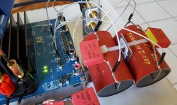
I finally managed to find some nice quality caps to replace the onboard DC blocking with ceramic cap and try to evaluate the effect on the sound quality of my precious TPA3251EVM.
I made this test very quick. I will think later how this can be assembled in a clean way. The ceramic caps were bypassed by soldering wires from exit of ceramic coupling caps until jumper headers for easier testing. There is absolutely no perceptible noise.
My first attempt was not successful. Sound was not meeting my expectations. Too flat, weak bass, shrunk sound stage. Was thinking switching back. But after overnight the stupid culprit mistake jumped into my face. The header pins I choose for the bypass were connected on both sides of the coupling ceramic cap, and this certainly messed the sound. After changing to the header pins linked to AIB and switching on again, the awaited wow effect came.
I like the "out of the box" sound of this board very much. It is really good. There is some kind of graininess I like on some tracks, like vocals but disturbs me on others like orchestral passages where it becomes a bit harsh like the big grains are blocked in the audio tube. Compared to my modified amps, the sound stage is very nice and precise but smaller, more around the speakers.
The replacement of the ceramic caps by nice big red Jantzen, bypassed by Wima fkp1 remove partially this graininess. To my opinion, highs have more details (grains are smaller), voices are more realistic and sound stage appears more consistent, bigger. Music seems to me more fluid. Complex passages are easier for me to follow and I feel bass to have more precision and pressure. And this is just with a few hours of burning in the caps on the counter.
I think this coupling modification (and input stage bypass) pushes this already very good amp board to a better level of musicality. It costs, beside the expensive caps, also half of the amps power. Ideal-wise a dac with balanced output is better with this amp. In my system it is a worth tweak. I will not go back.
I was thinking the coupling ceramic caps are directly connected to input pin of tpa3251, but I noticed while measuring that on this tpa3251evm there is still a 100Ohm resistor between them and input pins of chip (with 100pF to ground). This is certainly a LPF just before the pins. Soldering my wires on via inputs would have also bypassed this. I hesistate, but didn't do.
Dominique


Last edited:
The AIB pins do not bypass the ceramic coupling caps. They bypass the electrolytics and opamp stage. The 100R+100p are an LPF to filter out-of-band-noise which may cause additional heating due to oscillation or similar effects.
The AIB pins do not bypass the ceramic coupling caps. They bypass the electrolytics and opamp stage. The 100R+100p are an LPF to filter out-of-band-noise which may cause additional heating due to oscillation or similar effects.
In original state, yes, but the 2 wires will do the bypass, from J34 pin 3 to exit C17 and from J26 pin3 to exit C55.
Dominique
As I understand it, since there will always be zero volts across C28 and C63, there was no need to bypass them. You only needed the new caps to "replace" C17 and C55. If you were to go with a balanced input, you would have to "replace" C28 and C63. Two's company, four would be a crowd!
Nice work!
Mike
Just wondering if anybody has tried to replace those opamps - I guess with adequate soldering skills and/or daring it can be done.
I have a 3251EVM connected to a Mean Well LRS 350-36. I immediately get an OTW fault when resetting. I've played around with grounding, but maybe not correctly. I've also adjusted the output voltage, with no change. Any ideas are appreciated?
hi lima3
during the experts are talking 😀
i found this: page 15 #150
What is wrong with TPA3255?
chris
- Home
- Amplifiers
- Class D
- TI TPA3255EVM