Good day all,
I have a S/500, s/n: D87090454, that has an issue. Specifically, the middle of the right side heat sink gets much hotter than the same section on the left side. I saw there were schematics for the S/550 posted and I'm wondering how different the two units are. The one I have is an 'Optical bias' unit. I have to check the offset to see if there is a glaring difference. Going to open it up and test the outputs and resistors to see if they are all ok. Anyone have any other suggestions?
Thank you for any suggestions.
D
Ok, here's what I have so far, and I promise pictures will follow.
Output offset L: 2mV
Output offset R: 19.2mV
Voltage drop across L emitter resistors: all in the range of 72-80mV
Voltage drop across R emitter resistors: all in the range of 126-146mV
It looks like the outputs are being driven hotter across the board so I'm now looking at the small input circuit board as the source of my troubles.
Diagram anyone? Or suggestions?
if they're all inside that range , then electrically everything is OK , and temp difference must have culprit in mechanical domain*
key word is middle in your post #1
thermal goo is Dodo;
that means that you need to dismantle all output transistors , clean thoroughly (degrease also ! ) their cases and T Al bar of old thermal goo , same goes for mica thermal pads ; if some are suspicious/cracked , put new instead , but choose/buy ones of tinier variety
then put new (tiny!!) layer on both sides of (all ) mica thermal pad(s) and mount transistors back
considering physical layout of amp , it's best to start dismantling T bar from heatsink , then perform cleaning and re-gooing of transistors one by one , which will prevent possible mixup of their position
that's step 1 , pretty important ;
*step 2 is main reason for uneven temp. at heatsinks - most certainly uneven thermal contact (physical pressure , as measure of goo condition and screws tightening (between T Al bar and heatsink) )
you can cure that easily - for step 1 - you already unscrewed all bolts holding together T Al bar to heatsink ; clean old thermal goo from both sides ( T bar and heatsink) , degrease everything ; put thin layer of new thermal goo ; put T bar back , tighten all screws evenly.
Iq difference between channels (judging by voltage across emiter resistors) can be explained by time factor , nothing else , and it's easily settable ;plenty of schematics and info for that , floating in forum
however - if you think that's too much for you , feel free to send that bad amp to OPLDF
Attachments
Last edited:
regarding schematic , I believe you'll find something here :
http://www.diyaudio.com/forums/pass-labs/253789-threshold-s-550-a.html#post3872948
Nelson Pass related | Zen Mod Blog
http://www.diyaudio.com/forums/pass-labs/253789-threshold-s-550-a.html#post3872948
Nelson Pass related | Zen Mod Blog
Thank you for the info on where to begin.
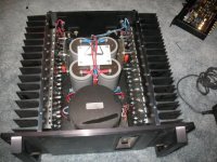
There is a single trim pot on the small input / bias circuit board. Is that an input trim or is that for bias?
Here are some shots of my amp.


There is a single trim pot on the small input / bias circuit board. Is that an input trim or is that for bias?
Here are some shots of my amp.
am I blind , or I can't see where pot is .... ?
😉
however - it must be for Iq , what else .....
easy to test - one DVM across output terminals , second DVM across one emiter resistor , fiddle with it slightly and you'll see what is happening
but - I advise to do that after entire procedure explained in my previous post
maybe Pa will chime in with more info , in a meantime
It's a small square white trim pot in the back left, behind the green cap on the input/bias board.
After I clean and lightly re-goo I'll fiddle about with it.
Thanks.
After I clean and lightly re-goo I'll fiddle about with it.
Thanks.
Hi all,
I know it's been a long time that I've checked in.
I reseated and resoldered all the output transistors on my S/500.
New development. It's popping Negative Rail fuses on the side I worked on.
All the transistors test good. All the resistors test good.
I'm at my wits end because I can't seem to locate the problem and I'm chasing my tail.
Anyone near NJ that works on these things?
I'm throwing in the towel.
I've fixed a lot of stuff over the years but this one has me bested. Maybe I'm just getting old.
Thanks for all the help.
- Status
- Not open for further replies.
- Home
- Amplifiers
- Pass Labs
- Threshold S/500 issue and circuit request.