Nickkuk,
Is claiming me that using the mosfet will not work, even if the simulator giving me the green light?
Is claiming me that using the mosfet will not work, even if the simulator giving me the green light?
I'm beginner too - I've just been modelling large 6000uF 450V caps on a toroidal etc as part of my amp's power supply. The inrush was up to 150A hence controlling the inrush through the to the main res cap.
Have you had a look at the current flowing through L1 on startup caused by the inrush to C1?
Controlling C1 with a mosfet would mean that 150A is spread over time and can be kept in line with the current limits of the transformer and the diodes. However it means that mosfet needs to cope with the power dissipation as heat.
I think Basreflex's point is that C2 sees the same low impedance (the Ron is some but not a lot) at start up.
It may not be a problem given the power is quite low but it may be inrush is larger than you think causing something to go bang. Either that or you may have to put up with a nice transformer inrush buzz when you hit the switch 🙂
Remember a model allows you to get away with things that would cause a real world system to fail with a bang, cause it to make nasty noises or fail over time. Especially in the thermal area - a component may say it can cope with 150W, however that's with perfect heat dissipation, so you need to consider the junction temperature and the imperfect cooling that will cause that junction temp to rise over time and so that 150W would be lower. Also inrush causes stress on components, so you may need to select larger components to cope reliably with it.
Last edited:
NickKUK
I will make a provisional assembly to test the mosfet. I will post the result here.
The inrush to C1 is no problem for the toroid.
I will make a provisional assembly to test the mosfet. I will post the result here.
The inrush to C1 is no problem for the toroid.
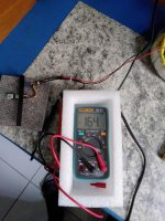
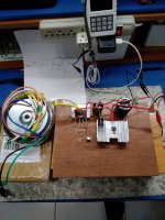
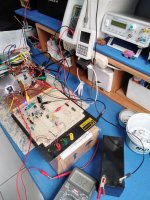
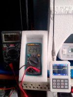
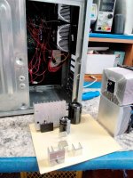
Individual test of the IRF6218 mosfet. (okay)
To clarify any doubts, if the component is fake, I tested the zener voltage (164v) and submitted it to a power of 75w for 1 hour. I used a computer heatsink. as you can see in the photo.
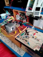
Assembly
As you can see in the photo, I decided to weld all the components, leaving no scope for any contact failure.
Sink dimensioned to 10w (0.130R * 7A * 7A = 6.37w)
0.6A primary fuse
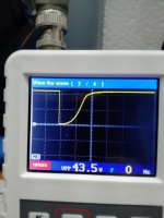
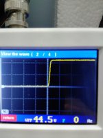
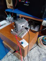
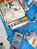
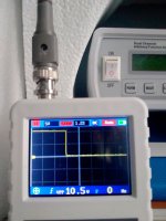
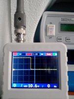
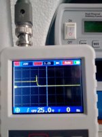
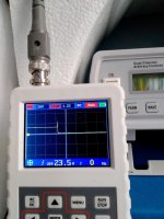
Inrush test. (okay)
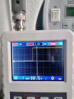
As shown in the photo, with the oscilloscope in the scale of 1.2s/div, the capacitor is charged in 200ms (exactly as in the simulator). In the other photo, with the oscilloscope in the 100ms/div scale, it shows the curve better.
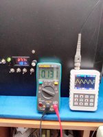
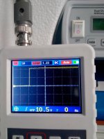
Test of Rds (on) and ripple. (okay)
As attached photo, with a load of 1A we have the Vds reading of 0.130v (which is equivalent to 0.130R). We have also displayed the Ripple voltage at the output.
Transistor Q1(bc557) discharging C2. (okay).
Observe in the photo, the quick action of q1(bc557) on the voltage of C2(470uf), preventing problems in the off/on.
Rds (on) for i-sense. (disapproved).
It showed small variations as a function of temperature.
To clarify any doubts, if the component is fake, I tested the zener voltage (164v) and submitted it to a power of 75w for 1 hour. I used a computer heatsink. as you can see in the photo.
Assembly
As you can see in the photo, I decided to weld all the components, leaving no scope for any contact failure.
Sink dimensioned to 10w (0.130R * 7A * 7A = 6.37w)
0.6A primary fuse
Inrush test. (okay)
As shown in the photo, with the oscilloscope in the scale of 1.2s/div, the capacitor is charged in 200ms (exactly as in the simulator). In the other photo, with the oscilloscope in the 100ms/div scale, it shows the curve better.
Test of Rds (on) and ripple. (okay)
As attached photo, with a load of 1A we have the Vds reading of 0.130v (which is equivalent to 0.130R). We have also displayed the Ripple voltage at the output.
Transistor Q1(bc557) discharging C2. (okay).
Observe in the photo, the quick action of q1(bc557) on the voltage of C2(470uf), preventing problems in the off/on.
Rds (on) for i-sense. (disapproved).
It showed small variations as a function of temperature.
Attachments
-
 20210324_092948_2.jpg743.5 KB · Views: 174
 -
 20210325_190823_2.jpg650.2 KB · Views: 90
 -
 20210325_180033_2.jpg407.1 KB · Views: 90
 -
 20210325_180015_2.jpg517.3 KB · Views: 160
 -
 20210325_175957_2.jpg379.7 KB · Views: 164
 -
 20210325_175654_2.jpg677 KB · Views: 168
 -
 20210324_144508_2.jpg609.3 KB · Views: 169
Hi
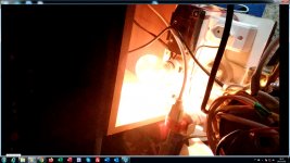
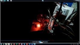
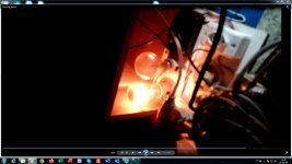
Using a series lamp with the transformer, it was possible to observe the performance of the Mosfet, in the starting smoothing.
Image 1: Observe the intense brightness, without using the Mosfet (total capacitance of 26700uf).
With the use of the Mosfet, the start was divided into two stages: the first with the 4700uf capacitor (image 2). After 1s the second stage happens, with the mosfet releasing the capacitor charge of 22000uf (image 3).
Attachments
Hi
Finally the Max4080 arrived. God, how small it is! I had to improvise (image 1), because I don't have an adapter base.
It worked really well! I was a little concerned with the speed of response but passed the tests well. I shorted the output a hundred times, in several current setups.
Finally the Max4080 arrived. God, how small it is! I had to improvise (image 1), because I don't have an adapter base.
It worked really well! I was a little concerned with the speed of response but passed the tests well. I shorted the output a hundred times, in several current setups.
Attachments

that maxim chip is big, i once had to solder wires to realtime clock chip 1.27x1.9mm. WLCP9, PCF8564...
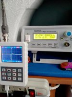
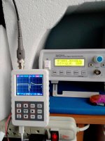
Today was the day to perform tests with a 12v battery.
Test 1 - connecting the battery to the input terminals, with the PSU off.
The defense system (d5, d6, d7, d11, m2, q6) worked perfectly! The big expectation was with the max4080, as it is not bidirectional. A high current would pass through resistors r5 and r6, considerably increasing the voltage (reversely) on pins 1 and 8. D11 was then implemented, with the purpose of keeping the potential difference low between pins 1 and 8 and offering passage to the rest current to the capacitors. It worked, and the max4080 survived. Observe in image 1, a current (38.9ma) drained from the battery, mainly coming from the current source (q11).
Test 2 - charging the battery (image 2), turning off the PSU in the middle of the process.
Defense system (d5, d6, d7) worked perfectly and nothing was affected.
Test 3 - battery connected to the input terminals with psu at 5v.
Once again the defense system (d5, d6, d7) worked perfectly and nothing was affected. Removing the battery, return to 5v.
Attachments
Hi
With the max4080 I am able to control very small currents. Notice in image 1, a current of 20ma being applied to a 1.5v battery, providing a slow charge.
I made an update of the project, inserting the indicative led (image 2)
The other part of this project, you can follow in this other topic:
Adjustable power supply from 1 to 30v with the LM723 + TL7660 + LM336
Attachments
Hi
The project has an excellent output stability, at the time of activation / deactivation of the psu.
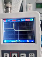
Image1 (start): Construction of the perfect output voltage when starting the PSU. Output configured for 10v, without load.
image 2 (start): Construction of the perfect output voltage when starting the psu. Output configured for 10v, using load (1A).
image 3 (off): Output voltage declines very fast. Without load.
image 4 (off): Presenting the same behavior in the decline, using a load of 1A.
image 5: now using a current limitation of 40ma (output voltage at 10v). Using an LED on the output with the resistor of a 1R in series. Oscilloscope positioned to read the resistor voltage. The idea here was to analyze the max4080, if it would react quickly when starting the psu. Observe on the oscilloscope that the reaction was excellent, without any peak at startup. The LED is safe (image 6).
The project has an excellent output stability, at the time of activation / deactivation of the psu.
Image1 (start): Construction of the perfect output voltage when starting the PSU. Output configured for 10v, without load.
image 2 (start): Construction of the perfect output voltage when starting the psu. Output configured for 10v, using load (1A).
image 3 (off): Output voltage declines very fast. Without load.
image 4 (off): Presenting the same behavior in the decline, using a load of 1A.
image 5: now using a current limitation of 40ma (output voltage at 10v). Using an LED on the output with the resistor of a 1R in series. Oscilloscope positioned to read the resistor voltage. The idea here was to analyze the max4080, if it would react quickly when starting the psu. Observe on the oscilloscope that the reaction was excellent, without any peak at startup. The LED is safe (image 6).
Attachments
Last edited:
Hi
I decided to implement a safety system, in case the power transistor suffers a short circuit.
image 1: 10v output voltage, with 1A load. Closing short between collector and emitter.
image 2: 10v output voltage, without load. Closing short between collector and emitter.
image 3: Start psu with collector and emitter shorted. Without load resistor.
image 4: Start psu with collector and emitter shorted. with 8R load resistor at the output.
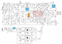
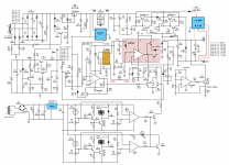
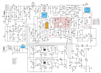
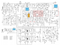
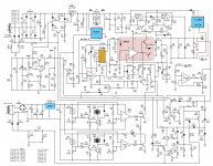
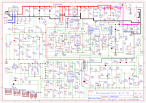
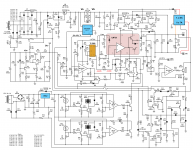
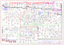
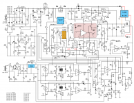
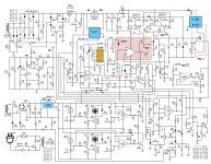
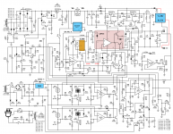
image 5: Updated schematic.
I decided to implement a safety system, in case the power transistor suffers a short circuit.
image 1: 10v output voltage, with 1A load. Closing short between collector and emitter.
image 2: 10v output voltage, without load. Closing short between collector and emitter.
image 3: Start psu with collector and emitter shorted. Without load resistor.
image 4: Start psu with collector and emitter shorted. with 8R load resistor at the output.
image 5: Updated schematic.
Attachments

MCP6002
I had a problem with the regulation of the CC, due to a limitation of the MCP6002. Due to the low value of the full-swing (30khz), the opamp output would turn off, before the full adjustment range. For example, for a 1.7A load, I was only able to get an adjustment from 0 to 0.8A. Exceeding 0.8 the opamp cut the output voltage, releasing the load to 1.7A.
Analyzing the graph (image 1), I could see that lowering the supply voltage to approximately 2v, could extend the full-swing considerably. To lower the voltage of the MCP, I used a blue led (LD7), as you can see in the schematic. The MCP6002 started to operate at 60khz.
I noticed that the MCP was trying very hard to keep things under control and so I decided to change the capacitor C22 (pin 13 of the LM723) from 1nf to 100nf and the magic worked. MCP started to operate close to 8.5 kHz, operating only on the pulse width. Observe in image 2, the CC set to 100ma (output voltage 14v with a load pulling 1.7A). See the oscilloscope at the base of Q5 showing the MCP operating at approximately 8.5Khz. Now look at image 3, where CC was set to 1A. The signal at the base of Q6 with the smallest pulse width, staying close to 8.5 kHz.
I decided to keep the MCP6002 operated with low voltage (2.1v), ensuring a high pull-swing.
Attachments

Hi!
Load Transient Testing
Today was the day to choose the output capacitor. As a parameter, I stipulated that the peak-to-peak voltage (between the overshoot and the undershoot) was a maximum of 8% (load at 2A), for the output voltages of 5v and 3.3v. I started with a 100uf capacitor but the one that best met the parameter was 220Uf.
Image 1:
- 1khz frequency (pulse set to 100us)
- 3.3v output voltage / 2A load current
Image 2:
- 1khz frequency (pulse set to 100us)
- output voltage 5v / load current 2A
Image 3:
- 1khz frequency (pulse set to 100us)
- output voltage 20v / load current 2A
Attachments

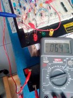
Protection system and the use of batteries in the output terminals.
Due to the protection system, in the event of a short-circuit of the power transistors, I had to insert an additional protection, for charging my batteries.
Test 1 - connect the battery to the input terminals, with the PSU off.
With the battery's own energy, the SCR TR3 is activated, keeping the MOSFET M1 (IRF6218) in the cut. The PSU will only turn on fully when the battery is removed from the terminals. See in image 1, that there will be a consumption of 64ma of the battery.
Test 2 - charging the battery, with the PSU shutdown in the middle of the process.
SCR TR3 will also be activated here, blocking the M1 Mosfet. The PSU will only turn on fully when the battery is removed from the terminals.
Test 3 - battery connected to input terminals with psu at 5v.
Once again the defense system (d5, d6, d7) worked perfectly and nothing was affected. Removing the battery, return to 5v.
Follows the updated scheme.
Attachments
Finished Tests:
CRCRC filter: Very good.
Soft Start: Very good.
Filter with capacitance multiplier for Lm723: Very good.
CV with low output noise: Good (It will be even better with the PCB and adequate cabling).
CC: Good.
Load transient:Very good.
Quick shutdown of PSU - short-circuit power transistors: Good.
Cooling system, with limit temperature protection: Very good.
Construction of the output voltage, when turning on the PSU: Very good.
Quick deconstruction of the output voltage, when turning off the PSU: Very good.
Next step: building the pcb
Hi
Follows schematic, with some corrections in the project. Follow the link to open it in the digkey application.
Lm723_Digkey
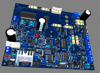
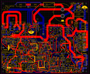
I will assemble the PCB by EasyEDA. Follows schematic and file.
Follows schematic, with some corrections in the project. Follow the link to open it in the digkey application.
Lm723_Digkey
I will assemble the PCB by EasyEDA. Follows schematic and file.
Attachments
OVP (overvoltage protection).
I replaced the monitoring of the VCE voltage of the power transistors, by a more elaborate circuit, which was capable of causing the least possible damage to the DUT. I used a comparator (Lm393) to be monitoring the input value (pin 5) with the output voltage, because the Lm723 is working with a fixed gain. With the potentiometer P8 it is possible to adjust the percentage of the allowed overvoltage (I set it to 10%).
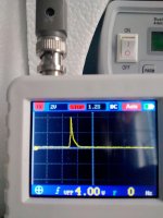
Observe the image 1. Output set to 5v. With an external power supply set to 5.8v, I forced the voltage to rise at the output terminals. The OVP kicks in, shutting down the PSU.
Image 2 - Output configured for 12v, with load at 2A. I caused a short circuit between collector and emitter of the power transistor, throwing the 40v in the output. The OVP kicks in, cutting off the supply.
When LM393 detects overvoltage (10% above Vout), it activates the SCR (tr2), which turns off the Mosfet M1 (IRF6218), interrupting the supply. In sequence, the SCR (tr1) is activated, discharging capacitor c7 (22mUF).
I replaced the monitoring of the VCE voltage of the power transistors, by a more elaborate circuit, which was capable of causing the least possible damage to the DUT. I used a comparator (Lm393) to be monitoring the input value (pin 5) with the output voltage, because the Lm723 is working with a fixed gain. With the potentiometer P8 it is possible to adjust the percentage of the allowed overvoltage (I set it to 10%).
Observe the image 1. Output set to 5v. With an external power supply set to 5.8v, I forced the voltage to rise at the output terminals. The OVP kicks in, shutting down the PSU.
Image 2 - Output configured for 12v, with load at 2A. I caused a short circuit between collector and emitter of the power transistor, throwing the 40v in the output. The OVP kicks in, cutting off the supply.
When LM393 detects overvoltage (10% above Vout), it activates the SCR (tr2), which turns off the Mosfet M1 (IRF6218), interrupting the supply. In sequence, the SCR (tr1) is activated, discharging capacitor c7 (22mUF).
Attachments

Current Peaks Test
I recently read the article by experient Bram, about protection against strong peak currents (short-circuit output terminals), in which the opamp's of the CC are not able to react in time.
PSU Destroyer Mark I
I confess that in my countless short-circuit tests, I was using long cables. I carried out new tests with a 4mm cable and very short, and by the tenth short circuit the BD139 broke.
I then decided to implement a line of defense, for intense current spikes, using the LM723's transistor (pins 2 and 3). New tests and the problem has been solved.
Follows updated schematic.
Attachments
- Home
- Amplifiers
- Power Supplies
- Three functions for a Mosfet: CRC Filter, Soft Start and i-sense. Will it work or not