Hey,
I am building a class B BJT based amplifier. I have a couple of questions concerning the thermal tacking of the bias transistor. First of all, is it neccessary for the predrivers to be heatsinked? I am using MJE 340/350. If they need to be heatsinked then I will probably mount them to the same heatsink as the OP transistors which are TIP31/32's. I read that the bias transistor should be mounted directly to one of the predrivers but I am wondering if all of the aforementioned transistors should be thermally coupled (on the same heatsink). Is this the best way to go?
Thanks,
Mark
I think we may have some issues with semantics, I refer to the output devices as outputs and the devices that drive those as drivers. Are you calling what I call drivers pre-drivers?? If so, then many manufacturers mount the drivers on separate heat sinks from the outputs, then mount the bias tracking transistor to the output heat sink. This seems to work fairly well if the drivers have a significant bias current going through them at idle, which tends to keep them at a fairly steady temperature. As for my home build stuff I just mount everything on the same heat sink, seems to work too (works for chip manufacturers also, they don’t have a choice). If what you’re referring to as pre-drivers is the input device to a triple darlington, I don’t think anybody heat sinks those. A schematic of what you’re doing would be helpful.
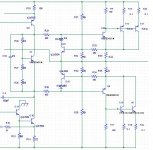
I’m guessing 15 volt rails? Don’t know what output bias current you’re planning on, but the .1 ohm resistors on the emitters of the outputs may be a bit low to promote sharing at idle. Matching outputs would probably be a good idea. Also, an output zobel will probably be needed for stability, though you may have that in a portion not shown.
I would put drivers and output transistors and bias transistor all on the same heat sink.
The heatsink should be around the average heat value of all the components.
The heatsink should be around the average heat value of all the components.
Heatsinking....drivers...etc...
For the amplifier schematic you posted, which is a CFP output stage it is not necessary to have the drivers and output devices on the same heatsink. I would also suggest upping the value of the .1 emitter resistors...a little insurance if you will.
I would suggest putting a heatsink on the driver transistors, to increase the thermal mass. I've built a CFP amplifier before where the voltage rails were low enough that power in the drivers wasn't that big of an issue. So I did not fit heatsinks to the drivers....the issue then became bias stability. Even with the bias transister epoxied with silver thermal epoxy to the driver the bias controller had a tough time keeping up with the rapid temperature changes. Some small ~20C/W heatsinks on the driver transistors were enough to slow the temperature rate of change down so the bias controller could keep up.
Scott
Thanks for all the replies so far they are really helpful. Koas the voltage rails are +/- 18v. Close to what you thought.
As for the 0.1 ohm resistors, what value would you guys suggest? Maybe .33 ohms? Actually I would like to go with a higher value because the 0.1 ohm resistors are hard to find. I purchased the metal film type (an actual strip of metal) and the leads are very thick which might make it hard to mount on pcb.
As for the 0.1 ohm resistors, what value would you guys suggest? Maybe .33 ohms? Actually I would like to go with a higher value because the 0.1 ohm resistors are hard to find. I purchased the metal film type (an actual strip of metal) and the leads are very thick which might make it hard to mount on pcb.
post three shows a CFP output stage.
The temperature compensation must monitor the driver (or pre-driver if used) temperatures.
Mount the two drivers and the Vbe multiplier on a common heatsink.
Mount the output devices on a separate and big heatsink.
CFP stages generally run a far lower bias current and traditionally run much cooler as a result, when used in the domestic situation.
If you're using 8ohm speakers and normal domestic SPLs, then you can get away with a very small output stage sink. Possibly as small as the aluminium backplate of the amp chassis with a 5C/W sink on the outside.
4mV across each of R35 and R36 may be sufficient, that's ~6mA through each of the output transistors and drivers.
You need a cap across the BE of both protection transistors.
Adding a base resistor before each cap connection will allow you to tune the peak current limit for fast transients.
- Status
- Not open for further replies.
- Home
- Amplifiers
- Solid State
- Thermal Tracking Question