Hello!
I don't know if I just dug an old disscusion. 😀
(I am trying to build power amp for woofers in 3-way systems with fully symmetrical topology and super complementary output stages).
The super complementary is consist of both Darlington and Sziklai arrangements. So it can't be compensated like individual arrangements. My question is: how can I get right thermal compensation for this arrangement?
I also wanted to know how Bryston designers can get compensation with only one mountable device (MJE180) in Vbe multiplier "stage"?
Thanks all for your concerns!
"Super Complimentary" surely it is either complementary or quasi complimentary. Where does "Super" fit in?
Hi Nikolai,
I believe, what you mean - is a Bryston type of output arrangement.
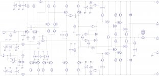
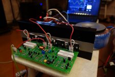
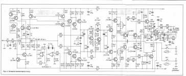
See my old project pictures attached. I used a 2-transistor bias spreader there, however only the bottom transistor (Q15) is placed on the main heatsink. The other one is just placed on the board. This prototype is still running nicely in my lab (since the end of 2013 🙂).
Let me know if you will have more questions.
Cheers,
Valery
I believe, what you mean - is a Bryston type of output arrangement.
See my old project pictures attached. I used a 2-transistor bias spreader there, however only the bottom transistor (Q15) is placed on the main heatsink. The other one is just placed on the board. This prototype is still running nicely in my lab (since the end of 2013 🙂).
Let me know if you will have more questions.
Cheers,
Valery
Attachments
Hi Nikolai,
I believe, what you mean - is a Bryston type of output arrangement.
See my old project pictures attached. I used a 2-transistor bias spreader there, however only the bottom transistor (Q15) is placed on the main heatsink. The other one is just placed on the board. This prototype is still running nicely in my lab (since the end of 2013 🙂).
Let me know if you will have more questions.
Cheers,
Valery
Thanks Valery.
Yes, Bryston type output stage. The solution you have shown is so simple 😀 I have thaught everything too complex like use two individual heatsinks with two thermal tracker lying on them... etc 😀
Ah, the drivers must have they own seperated heatsinks, correct?
My question maybe foolish 😀
In fact, a single main heatsink with all the outputs, plus the drivers, is enough - that's the way my prototype is arranged. It's thermally stable, can run for hours or several days at different output levels - no problem.
However - that would be kind of more "hi-end" implementation - you can place the drivers on a separate heatsink and even track its temperature with the top transistor in the spreader (NPN, connected as a diode).
Choosing the output transistors for this topology, make sure they are fast enough - so called RET transistors are what you'd want to look at (fT = 50MHz or so).
Sankens, like 2SC2922/A1216 or the newer ones 2SC3264/A1295, or NJW3281/1302 - would be a good choice. Transistors like MJ21193/21194 (fT = 4MHz) will most likely kill themselves in this arrangement - they're too slow while closing.
Did you mentioned "cross-conduction"?In fact, a single main heatsink with all the outputs, plus the drivers, is enough - that's the way my prototype is arranged. It's thermally stable, can run for hours or several days at different output levels - no problem.
However - that would be kind of more "hi-end" implementation - you can place the drivers on a separate heatsink and even track its temperature with the top transistor in the spreader (NPN, connected as a diode).
Choosing the output transistors for this topology, make sure they are fast enough - so called RET transistors are what you'd want to look at (fT = 50MHz or so).
Sankens, like 2SC2922/A1216 or the newer ones 2SC3264/A1295, or NJW3281/1302 - would be a good choice. Transistors like MJ21193/21194 (fT = 4MHz) will most likely kill themselves in this arrangement - they're too slow while closing.
But I have choose MJ21193/21194 for the design (I already have MJ21193/21194) 😱
Since the amp is fed by low-pass filter so I think at low frequency (<700Hz) the cross-conduction should not be a problem. And I also decide to create a wide safety margin, 4 MJ21193 and 4 MJ21194 for the output stage fed by +-56V. Will it survive the cross-conduction? 😀
And I will buy NJW0281/0302 for mid amp and FJP5200/1943 (good proved transistors?) in order to save money for the transformer and speaker sets(I haven't bought yet 😀 )
Thank you.

This work vas well done by Onkyo in 1996 with the amps A-9911/9711 and Integra 927.
Do you mis-post 😕 ? I am asking about the Bryston output stage, not the sziklai pair. 😱
Well, Bryston topology is somewhat... half-EF / half-Sziklai.
However, as my live tests have shown, the EF-type-of bias spreader with transistor, placed on the main heatsink, does the job well.
However, as my live tests have shown, the EF-type-of bias spreader with transistor, placed on the main heatsink, does the job well.
Well, Bryston topology is somewhat... half-EF / half-Sziklai.
However, as my live tests have shown, the EF-type-of bias spreader with transistor, placed on the main heatsink, does the job well.
Ah hah, the very tightly stability of bias current seem be not necessary in the amp that only operate in low frequencies, since there a lot of NFB. I have exaggerate everything 😀
Ah hah, the very tightly stability of bias current seem be not necessary in the amp that only operate in low frequencies, since there a lot of NFB. I have exaggerate everything 😀
Global NFB loop does not influence bias at all, so thermal feedback, arranged the right way if vitally important (thermal feedback is also an NFB, but it's 100% independent from the "signal" feedback loop). Otherwise, you end up with thermal runaway (and OPS self-destruction).
Global NFB loop does not influence bias at all, so thermal feedback, arranged the right way if vitally important (thermal feedback is also an NFB, but it's 100% independent from the "signal" feedback loop). Otherwise, you end up with thermal runaway (and OPS self-destruction).
No, I mean rich NFB at low freq can cancel more distortion cause by poor bias. Or I am wrong?
Crossover distortion - that's what you're going to experience with poor bias - is one of the most "evil" types of distortion. It adds unlimited number of new components, not correlated to the input signal. Lots of NFB will decrease overall level of distortion, increasing the number of unwanted components even more at the same time.
That's what some people call "transistor sound".
If you'd like to have a good-sounding amplifier, you need need to achieve as high linearity / low distortion open loop as possible, before applying the global feedback.
Optimal bias is one of the parameters on the way to achieving this requirement.
That's what some people call "transistor sound".
If you'd like to have a good-sounding amplifier, you need need to achieve as high linearity / low distortion open loop as possible, before applying the global feedback.
Optimal bias is one of the parameters on the way to achieving this requirement.
Crossover distortion - that's what you're going to experience with poor bias - is one of the most "evil" types of distortion. It adds unlimited number of new components, not correlated to the input signal. Lots of NFB will decrease overall level of distortion, increasing the number of unwanted components even more at the srame time.
That's what some people call "transistor sound".
If you'd like to have a good-sounding amplifier, you need need to achieve as high linearity / low distortion open loop as possible, before applying the global feedback.
Optimal bias is one of the parameters on the way to achieving this requirement.
Thanks.
When people had not discovered the cross-over distortion, a lot of listeners quickly concluded that transistors is inherent worse than valves. I think it is one of the largest regret in electronic technology. 😡 If not, we may be able to buy audio transistors cheapers now.
Ah, how can I decide the optimal bias?
(Many designers said that bias current should be 50-150mA per device, is it right?)
Bias is voltage. Of course, it leads to certain collector current, but still - bias is voltage. For BJT based push-pull output stage, optimal bias corresponds to 26mV over each emitter resistor for transistors at the output. See the well-known books by Bob Cordell and Doug Self for more details.
Cheers,
Valery
Cheers,
Valery
Optimal bias (of a BJT output stage) means minimising cross-over distortion.................
Ah, how can I decide the optimal bias?
(Many designers said that bias current should be 50-150mA per device, is it right?)
One wants this to be consistent for operating conditions where the outputs and drivers change temperature.
Optimal bias is a voltage, not a current.
One tries to set the bias voltage and adjust the bias voltage to maintain that lowest cross-over distortion.
~26mVre is the optimum for an EF stage operating at room temperature. This increases as the Tj increases above room temperature.
But there is a complication, the mVre includes both the voltage across the external emitter resistor and the internal emitter resistance of the transistor. One cannot easily measure the Vre(internal). Instead one sets up the Vbias using the measured crossover distortion.
Bias is voltage. Of course, it leads to certain collector current, but still - bias is voltage. For BJT based push-pull output stage, optimal bias corresponds to 26mV over each emitter resistor for transistors at the output. See the well-known books by Bob Cordell and Doug Self for more details.
Cheers,
Valery
Optimal bias (of a BJT output stage) means minimising cross-over distortion.
One wants this to be consistent for operating conditions where the outputs and drivers change temperature.
Optimal bias is a voltage, not a current.
One tries to set the bias voltage and adjust the bias voltage to maintain that lowest cross-over distortion.
~26mVre is the optimum for an EF stage operating at room temperature. This increases as the Tj increases above room temperature.
But there is a complication, the mVre includes both the voltage across the external emitter resistor and the internal emitter resistance of the transistor. One cannot easily measure the Vre(internal). Instead one sets up the Vbias using the measured crossover distortion.
Thanks for info.
(I asked for "bias current" beacuse the emitter resistor is fixed at 0,24Ohm, sorry because I haven't mentioned the resistor value 😀 )
But how can I measure cross-over distortion? I don't have an accuracy oscilloscope. Is there any way to turn my computer into an acurracy oscilloscope? 😕
use the approximate method of setting Vre to about 26mVre.
If you have a high Re then it swamps the internal Re and you set 26mV on the external.
If you reduce Re, then a higher proportion of the total Vre appears across the internal, so you have to guess at the optimum external Vre.
By the time you get down to 0r1 external, you may have only 18 or 19mVre across that value. For 0r24 maybe aim for 22mVre.
- Status
- Not open for further replies.
- Home
- Amplifiers
- Solid State
- Thermal compensation for super complementary output stage?