Hi, everyone !
Throughout my youth I researched and designed class AB high-power audio amplifiers. I don't know why I did this... 😆 because I don't need hundreds of Watts of power to listen to music. And it doesn't make sense to power up a monster amplifier just to listen at a few Watts, which is more than enough for me. It also takes a lot of space. I don't like class A either because of it's high consumption, and neither chip amps. So I thought, what if I convert one of my power amplifier schematics into a small, miniaturized amplifier with SMDs ? I want to make it as small as possible, and as good as it gets.
And I came up with this schematics. 🙂
It is based on my high power amplifiere of 200W, which I already buid it, and it still works perfectly after 15 years of stressfull conditions in a comercial business of a friend of mine.
You can see it on my website: https://marus-gradinaru.42web.io/Audio/ZAL200V3/main.html

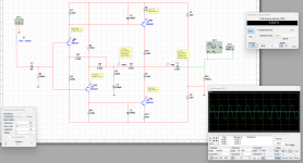
So, this new schematic it is powered at +/-16V must deliver 7W into 8R and 15W into 4R with 1Vrms imput signal. You can see the simulated parameters in the top-left of the image. Because the years have passed and I've forgotten a lot of what I studied about audio amplifiers, I want to talk to you before building it to make sure I didn't do anything wrong. First of all, I would like to discuss about the transistors used... Remember, they all must be SMD components (except for the power ones, obviously) !
The input stage.
In the input stage the most important is the noise factor of the transistors. And a bonus will be if they are a matched pair (NPN+NPN and PNP+PNP). As strange as it may seem, I haven't been able to find any decent low-noise transistors pairs in SMD package. The closest to what I want are the BCM847DS and BCM857DS. They say that the noise figure is 3dB typical. Will this be audible without music ? It is said that only the 10K volume potentiometer generate about 12.9 nV/√Hz, so it will ruin any low-noise transistor anyway... I don't know what to say... If you know a smd package with two NPN and two PNP matched transistors with lower noise than 3dB, that will not cost a fortune and they can be found easely, please let me know. But I think the chances are small, because I've already read here and haven't found anything suitable.
VAS stage.
In the VAS stage, as I remember, the most important is the Cob of the transistors. The Cob of the first transistor is more important than the second one, but they all needs to be low.
The BC847-857 has 1.5pF and 4.5pF. They are low enough, but I don't know how bad is if they are not the same.
The BCX56-53 has 4.5pF and 7pF. Still a little different...
In the simulation, the slew rate seems symmetrical, around 8-9V/us...
Output Stage.
Here, I selected the BCP56-56 as drivers.
In simulation, at maximum power, there are some 40mA current peaks and the average dissipated power is 120mW. The transistors are rated for 1A and 1.5W, so I gues they will do, right?
For the power output I thought about using MJE15030-31, which I used in my high-power amplifiers as drivers. I know they are not made for this, but do you think it will work for this little amp ? The transistors are rated for 8A and 50W. The peak output current in 4 ohms is 3A per transistor, and the average dissipated power per transistor si 6W max. Do you think they will hold ?
Another disadvantage would be that the gain is a bit nonlinear:
NPN hFE: 150 @0.7A / 100 @2A / 75 @3A
PNP hFE: 150 @0.7A / 120 @2A / 83 @3A
Will this matter much ?
I would be interested if you know of other more suitable output transistors, but only in the TO-220 package.
Throughout my youth I researched and designed class AB high-power audio amplifiers. I don't know why I did this... 😆 because I don't need hundreds of Watts of power to listen to music. And it doesn't make sense to power up a monster amplifier just to listen at a few Watts, which is more than enough for me. It also takes a lot of space. I don't like class A either because of it's high consumption, and neither chip amps. So I thought, what if I convert one of my power amplifier schematics into a small, miniaturized amplifier with SMDs ? I want to make it as small as possible, and as good as it gets.
And I came up with this schematics. 🙂
It is based on my high power amplifiere of 200W, which I already buid it, and it still works perfectly after 15 years of stressfull conditions in a comercial business of a friend of mine.
You can see it on my website: https://marus-gradinaru.42web.io/Audio/ZAL200V3/main.html
So, this new schematic it is powered at +/-16V must deliver 7W into 8R and 15W into 4R with 1Vrms imput signal. You can see the simulated parameters in the top-left of the image. Because the years have passed and I've forgotten a lot of what I studied about audio amplifiers, I want to talk to you before building it to make sure I didn't do anything wrong. First of all, I would like to discuss about the transistors used... Remember, they all must be SMD components (except for the power ones, obviously) !
The input stage.
In the input stage the most important is the noise factor of the transistors. And a bonus will be if they are a matched pair (NPN+NPN and PNP+PNP). As strange as it may seem, I haven't been able to find any decent low-noise transistors pairs in SMD package. The closest to what I want are the BCM847DS and BCM857DS. They say that the noise figure is 3dB typical. Will this be audible without music ? It is said that only the 10K volume potentiometer generate about 12.9 nV/√Hz, so it will ruin any low-noise transistor anyway... I don't know what to say... If you know a smd package with two NPN and two PNP matched transistors with lower noise than 3dB, that will not cost a fortune and they can be found easely, please let me know. But I think the chances are small, because I've already read here and haven't found anything suitable.
VAS stage.
In the VAS stage, as I remember, the most important is the Cob of the transistors. The Cob of the first transistor is more important than the second one, but they all needs to be low.
The BC847-857 has 1.5pF and 4.5pF. They are low enough, but I don't know how bad is if they are not the same.
The BCX56-53 has 4.5pF and 7pF. Still a little different...
In the simulation, the slew rate seems symmetrical, around 8-9V/us...
Output Stage.
Here, I selected the BCP56-56 as drivers.
In simulation, at maximum power, there are some 40mA current peaks and the average dissipated power is 120mW. The transistors are rated for 1A and 1.5W, so I gues they will do, right?
For the power output I thought about using MJE15030-31, which I used in my high-power amplifiers as drivers. I know they are not made for this, but do you think it will work for this little amp ? The transistors are rated for 8A and 50W. The peak output current in 4 ohms is 3A per transistor, and the average dissipated power per transistor si 6W max. Do you think they will hold ?
Another disadvantage would be that the gain is a bit nonlinear:
NPN hFE: 150 @0.7A / 100 @2A / 75 @3A
PNP hFE: 150 @0.7A / 120 @2A / 83 @3A
Will this matter much ?
I would be interested if you know of other more suitable output transistors, but only in the TO-220 package.

Nice. In case of input stage npn/pnp mismatch (DC offset due to difference in Vbe), how stable is VAS current vs. input DC offset? This should be easy to simulate.
Last edited:
@Terry2000 They have 7dB noise figure (more than 3dB) and are not SMD transistors... 😕
@radu2326 I am too old to change the topology now... I will work only to improve my current schematics.
@PMA How can I vary the DC offset to measure the VAS current ? If I change one of the 180R resistors from the differential emitters, the DC offset increase from 8mV to 30-40mV and, indeed the VAS current changes in both VAS transistors...
Just add 1 - 5 mV DC source in series with base or emitter of one of the input transistors (Q1 or Q2, any of them).
They are also available SMD. Over 3dB unfortunately. The match very tightly in my SPICE sim which I like about them.They have 7dB noise figure (more than 3dB) and are not SMD transistors...
With only 5mV in series with the Q1a base, the offset at the output changes with 3mV, and the change in current of VAS is insignificant.Just add 1 - 5 mV DC source in series with base or emitter of one of the input transistors (Q1 or Q2, any of them).
With 50mV, the offset changes with 20mV and the current of first VAS transistor changes with 0.3mA and the second with 3mA.
It is ok ?
It seems to be OK, if also idle current change of the output transistors is negligible. This is the key, the stability of output pair idle current.
if also idle current change of the output transistors is negligible.
At 50mV input DC offset the idle current of output pair changes with 20mA...
But why would DC offset appear on the input if it the audio signal is coupled through a capacitor ?
It is not the point. DC input voltage is pointless. The point is in Vbe voltage difference between individual transistors of the input quadruple Q1a,b , Q2a,b . In simulation, Vbe of a,b transistors is the same. In a real world, it is not. In your simulation, you have to add a DC source of several mV in series with base of only one transistor and then check stability of output pair idle current. Your topology may be sensitive to input transistors Vbe mismatch.
That's why I decided to go with matched pair for the input stage.Your topology may be sensitive to input transistors Vbe mismatch.
But the Vbe must be the same for all 4 transistors (NPNs with PNPs), or just between the NPNs and separately PNPs ?
You have the circuit in the simulator, it would take you less time to check then reading and writing at the forum. And you will also get better answer this way. The goal is to prevent possible temperature related issues that would reflect in ΔVbe. I have nothing more to add. Take or leave, try or not. It is your design.
in general, is it just the idle current of the output transistors that matters here, or are there effects in the VAS that should be observed as well when doing this sort of check?It is not the point. DC input voltage is pointless. The point is in Vbe voltage difference between individual transistors of the input quadruple Q1a,b , Q2a,b . In simulation, Vbe of a,b transistors is the same. In a real world, it is not. In your simulation, you have to add a DC source of several mV in series with base of only one transistor and then check stability of output pair idle current. Your topology may be sensitive to input transistors Vbe mismatch.
Their role their is to reduce the speed of transistors and make a softer sound by decreasing rise and fall time.
R14, R15, R25, and R26 are not needed with the lower-voltage rails.
ETA: Removing R25 and R26 requires adding clamping diodes in parallel with C6 and C7.
Ed
Great ! I removed R14 and R15 and it works fine.
But if I remove R25 and R26, then I connect the colectors of the VAS transistors directly to ground ?
And how I connect the clamping diodes in paralel with C6 and C7 ? And why ?
I though they were around 4db in To92 package. I used them in my 80w amp and get a 110db signal to noise ratio.
80w with 40v rails (36v) under full load.
I think this is the sweet spot that allows loud distortion free output with a pair of mosfets.
80w with 40v rails (36v) under full load.
I think this is the sweet spot that allows loud distortion free output with a pair of mosfets.
Yes, connect the collectors of Q5 and Q6 to ground. The diodes added in parallel to C6 and C7 should conduct only when the amplifier is clipping. They are needed to limit the current in Q5 and Q6 (without R25 and R26).But if I remove R25 and R26, then I connect the colectors of the VAS transistors directly to ground ?
And how I connect the clamping diodes in paralel with C6 and C7 ? And why ?
Another approach is to add transistors to limit the current.
Ed
I though they were around 4db in To92 package. I used them in my 80w amp and get a 110db signal to noise ratio.
Which transistors are you referring to ?
- Home
- Amplifiers
- Solid State
- The smallest audio amplifier for everyday listening (SMD, discrete, fully symmetrical, low power)