staggerlee said:
James/Salas,
First off the layout of this board is stunningly elegant. Just fantastic! Is this compatible with the schematic in post 1, which I believe is V1 with the R6 Mod?

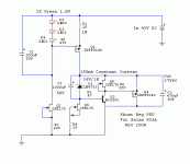
This one has R6 mod and is compatible.
Attachments
Tham said:Hi Iko,
Will try the version in post #456...for18Vdc output, do I change both the zeners to 18V diode? Any other changes need to be made?
For 18V output use a 10V and an 8V or two 9V. What is the load? According to the load you may want to change the 6R9 resistor. I used yellow LEDs with about 1.8V drop each, the least noisy I could find. Tell me more about the expected load current/circuit.
The DC input filter arrangements of normal B1 may compromise it. See to bypass them. It has 1 Ohm R1 in series. Here it kills your shunt's super low output impedance. Then it has C1,C2,C3. There it kills your shunt's bandwidth on 15.000uF of electrolytic and its ESR per divider's side. As it is, it is made to filter noise from wall wart psu's.
Hi Salas,
Any suggestion how to implement it with a normal B1? I have one already built with small (1000uF) filter caps.
Would this shunt regulator work better with your B1 design without output cap?
Any suggestion how to implement it with a normal B1? I have one already built with small (1000uF) filter caps.
Would this shunt regulator work better with your B1 design without output cap?
For normal B1, and to retain Iko's cascode and buffer version's benefits, delete R1, C1, C2.
If you have an input capacitor in your power amplifier or it has DC fault protection, there is a symmetric B1 with incorporated +/- shunts there.
If you have an input capacitor in your power amplifier or it has DC fault protection, there is a symmetric B1 with incorporated +/- shunts there.
An externally hosted image should be here but it was not working when we last tested it.
Hi Salas,
Can I connect the shunt output (18 or 24VDC) directly to the voltage divider of the normal B1 and remove altogether R1, C1, C2, & C3?
Can I connect the shunt output (18 or 24VDC) directly to the voltage divider of the normal B1 and remove altogether R1, C1, C2, & C3?
Tham said:Hi Salas,
Can I connect the shunt output (18 or 24VDC) directly to the voltage divider of the normal B1 and remove altogether R1, C1, C2, & C3?
Of course. That is what we are talking about.
P.S. How is your phono sound going on? Your shunt must have burned in and be mellower by now. You promised some pictures also.
Tham said:Hi Iko,
I am planning to use it to power a B1. Output can be 18 - 24VDC.
After you rectify and filter the input voltage, what does it measure to? What comes out of the transformer?
Honestly, for B1 I would use the v1 regulator. B1 barely draws any current. And definitely I second salas' point about the 1R input resistor, I would not use it with the shunt.
OK. Will build a new cascode and buffer version for the RIAA pre and use the V1 to power my B1 then. Will bypass R1, C1 & C2 as advised.
Salas said:For normal B1, and to retain Iko's cascode and buffer version's benefits, delete R1, C1, C2.
If you have an input capacitor in your power amplifier or it has DC fault protection, there is a symmetric B1 with incorporated +/- shunts there.
Wow, this is cool! Wasn't even aware of this thread, thanks salas!
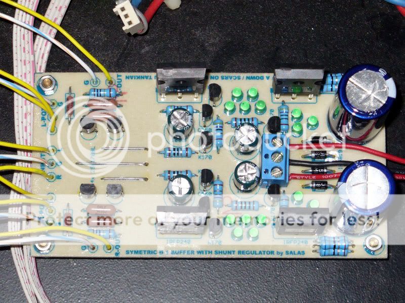
I am still trying to voice it...added another 2000uF of filter cap yesterday and more run in... hear fuller bass and more presence in the mid with this additional caps...may end up with 10000uF as suggested 🙂 .
Definitely photo will be forthcoming.
Definitely photo will be forthcoming.
Salas said:We also need to thank James for his PCB efforts.
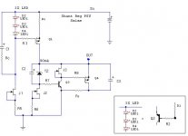
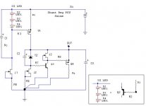
Here is his latest refinement for V1. He has included every possible nut n' bolt. LEDs CCS, Vbe CCS, positive / negative shunt, Zener socket for changing Vout in a sec, clean, compact, star layout. I did not see anything wrong by looking at it, you may have your second look too. James is more suitable to comment on the options and how to implement them I guess. He has also made a few V1s (not in WWII) and maybe he can convey his experiences and applications if he likes to.
Thanks again for your contribution James. 🙂
Hi Salas
I can not relate the connections in the pcb to your schematic... Does the pcb use several layers ?
😕
Ricardo

It should use only one layer.
Edit: the component numbering is a bit different than the schematic, since I think James was trying to accommodate both the version with PNP bias for the series mosfet, and the LED biased version.
Edit: the component numbering is a bit different than the schematic, since I think James was trying to accommodate both the version with PNP bias for the series mosfet, and the LED biased version.
Thanks DoDo,
Very neatly done - what program do you make/do the cct diagrams on?
The numbering system is top left to bottom right, just how you read a page - simple method for a simple mind!
Very neatly done - what program do you make/do the cct diagrams on?
The numbering system is top left to bottom right, just how you read a page - simple method for a simple mind!
Rs should go from shunt Mosfet's Drain to ground in the schematic, not between Drain and Q3's Emitter, thus breaking the ground. I prefer just a jumper there BTW. Its correct on the PCB.
I'm just wondering if anyone ran into these issues. Let's refer to v1 for now, say you finished it according to the pcb layout above. Now it needs to be coupled to the circuit you're powering. Let's even assume it's not a difficult load so you're not so worried about the output impedance; a phono stage like the salas RIAA draws something like 60mA, and it may vary a very few mA according to the music. Looking at the schematic at the you will see a few components connected to the series mosfet Q1: C2, TZ, J3, Q4, C3, OUT. Let's separate these according to function:
sensing: c2, TZ, J3
shunt action: Q4
filter: C3
load: OUT
Now, in the real world there may be a cable connecting OUT to the real load. Assuming this cable is AWG 18 (regular computer power cable thickness); the cable han approximate resistance of 6.4 mOhm/foot, or 200uOhm/cm. For a length of 20cm we get the equivalent of a 0.002R resistor between the regulator and the load. This cable may be soldered at its two ends, or maybe screw contacts are used. Well, this may add another two milliohms to this "virtual" resistor. What do you think this does to the output impedance measured at the load (i.e. how much does the voltage vary at the IN point of the load, if the current vary)? My simulation shows about 20dB loss in output impedance. And I did not even try for worst case scenarios. Most people probably do not use as thick a cable as AWG 18 for interconnections, right? Thinner cable will have higher resistance.
What to do about this. I have a solution but it's not yet tried in practice. Connect the sensing components with a separate cable directly to the IN point of the load thus splitting the current paths for sensing and shunting. Now the sensing components will try to control the shunt mosfet so that it regulates that point. In simulation this restores the output impedance to its previous levels. Pretty neat, eh?
Note: the transformer DCR (internal resistance), cable type, thickness, and soldering/crimping will be of major importance if the regulator feeds a larger load, such as a gainclone, or class D. Beware then of any resistance on the path going back from the load to the transformer/rectifier.
- Status
- Not open for further replies.
- Home
- Amplifiers
- Power Supplies
- The simplistic Salas low voltage shunt regulator