Going from balanced to unbalanced and back again???? Ha? I don't see any advantage........ excepting savings on switching and the attenuator....
Mark
Mark
I think USG3,4 in the rev2,3 is very different than the schematic of X2 rev0,1.
Rev2,3 in the manual, in page 1, it is stated that the input stage is Jfet driving MOSFET. In rev1 schematic it is only MOSFET differential.
Does anyone has the service manual / schematic for USG3,4?
Hi, Algar,
From your photograph, is it photograph of X2 or power amp?
In the moduls, they all seems to have 8 transistors (are they mosfets?) on each board, while X2 needs only 3 mosfets for 1 modul.
And also, in the center, between 2 pots, is it K389 Jfet? If it is, maybe it is what is talked in rev2,3
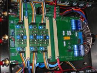
It was just to demonstrate the new small module approach used in the new Pass Labs product. This is the image of an amp not the actual X2 preamp. And donèt have more info on this image. I got it from this forum somewhere.
Bye...
Bye...
UGS stands for "universal gain stage" which is a complementary
set of match Jfets, cascoded, and driving level shifters. The
package uses parallel connector sockets which gives access
to the internal nodes. We use it everywhere except the highest
power amplifiers, where the voltage is too high. The advantage
to it is that it neatly packages up the most critical parts in the
signal path, and allows easy swapping in production, and easy
service later.
You will note that we have not included the UGS circuit in the
manual, as it is still in production.
Algar_emi said:It is probably something like these modules shown in this PassLabs X-Amp
Lovely relay,the yellow one on the pic, DS2E ?
But those awfull Philips capacitor things !
Once I have a failed experiment. I'm trying to make a 3 stages power amp, with Jfet for differential and MOSFET for VAS.
The supply is low, only +/-15V, so I think I do not need cascode for the differential Jfets.
The Jfet that I have is 2sk30y. The suffix is Y, and when I tested the IDSS (with G-D tied together) with ampmeter, it is only 2mA for 1 Jfet.
Because the k30's IDS only 2mA max, I designed the differential with only 1mA CCS (0.5mA to each leg).
The VAS is P-MOSFET, IRF9610 without source degeneration. I use 7K5 for the differential's drop resistor, that drives the G-S of the mosfet. I know this is quite strange value, very big. But with small differential CCS (0.5mA to 1leg and about >3V drop needed for GS of IRF), 7k5 is the value.
The experiment fail, because the result is the power amp looses the highs/trebles. When I replace the IRF9610 with bipolar, TIP32C, the trebles are there.
I really wanted to make Jfet differential and VAS MOSFETS that works, but how to do it with 2mA IDSS K30Jfets for differential?
Is it not possible to use 2mA IDSS for differential that drives MOSFET VAS? OR the highs are missing because I dont put cascode? But why with bipolar VAS everything seems normal?
In the X2 owners manual the unbal and bal input impedance is given as 10K and 20K respectively. However, in the specifications at the end of the manual these numbers are given as 10k and 44K respectively. Which of these is right? Thank you all.
gl
gl
Simple question:
What is the value of VREF for version 1, is it 9v? Does anyone know the voltage across R308?
Thank you!
-David
What is the value of VREF for version 1, is it 9v? Does anyone know the voltage across R308?
Thank you!
-David
Across R308 there is not voltage . R308 is there to slow down the mosfet against parasitic oscillations , since its gate input impedance is very very high .
So the value of Vref is about -32+5+4 = -23
So the value of Vref is about -32+5+4 = -23
Nelson Pass . . .
Well, you know what a current mirror is - there are plenty of
examples on this site.
Can I call this a current mirror . . . ?
Attachments
- Status
- Not open for further replies.
- Home
- Amplifiers
- Pass Labs
- The Pass Labs X2 - service manual