Re: Re: Re: Re: Balnced Arrangement
Isn't this exactly what would happen with 2 series FF? (running on the same clock)
guido said:
It should not happen that the FF inputs are changing state at the same time as the FF is clocking the data
Isn't this exactly what would happen with 2 series FF? (running on the same clock)
Re: Re: Re: Re: Re: Balnced Arrangement
I think what is meant is that they do not run on same clock but one clock is inverted😀
But i can see from another post that the reclocking is already ongoing.
Bricolo said:
Isn't this exactly what would happen with 2 series FF? (running on the same clock)
I think what is meant is that they do not run on same clock but one clock is inverted😀
But i can see from another post that the reclocking is already ongoing.
Re: Re: Re: Re: Re: Re: Balnced Arrangement
No I was meaning 2 series FF running on the same clock
Like here:

guido said:
I think what is meant is that they do not run on same clock but one clock is inverted😀
But i can see from another post that the reclocking is already ongoing.
No I was meaning 2 series FF running on the same clock
Like here:
Hi!
One more- did somebody tried to trim the original schematic from D1 from Mr. Pass to 2V or little more to make it suitable for our TDA1543?
I build it as the schematic in the manual, and i can trim beween -3,2 and +1,9V. But you only need to change the 100k resistor to get more range.
HI!
Till -- thanks man for the answer. Could You also tell how it works ( better than passive if You are using TDA1543?). I use passive TDA1543 out (power supply is 7V and I/V is 2k2 and Vref 1k5) and it is working - oh my...! But I would like to make it even better...😀 😀
regards
daniel
Till -- thanks man for the answer. Could You also tell how it works ( better than passive if You are using TDA1543?). I use passive TDA1543 out (power supply is 7V and I/V is 2k2 and Vref 1k5) and it is working - oh my...! But I would like to make it even better...😀 😀
regards
daniel
I use the D1 stage with the AD1865 you can see in this thread:
http://www.diyaudio.com/forums/showthread.php?s=&threadid=33138
i had no time for tests with other DACs now.
I noticed after warm up its possible to trim to slightly > 2V as maximum.
http://www.diyaudio.com/forums/showthread.php?s=&threadid=33138
i had no time for tests with other DACs now.
I noticed after warm up its possible to trim to slightly > 2V as maximum.
O.k. - I will try to put 100k resistor little lower when I do that I/V - that should be good enough to trim it up to 2,1V.
I think that one of my friends would use it so I must ask...
regards
daniel
I think that one of my friends would use it so I must ask...
regards
daniel
Anybody has a hint what may be the reason for some THD coming out of D1 stage? I build left and right channel http://www.diyaudio.com/forums/showthread.php?postid=383834#post383834
independend if i connect the left or right DAC one gives me four times theTHD than the other. All voltage levels and current flow looks pretty the same on both. Are there components to match very good? Or is it a bad FET? i used IRF510 branded "SEC"
independend if i connect the left or right DAC one gives me four times theTHD than the other. All voltage levels and current flow looks pretty the same on both. Are there components to match very good? Or is it a bad FET? i used IRF510 branded "SEC"
Hi, Stefanobilliani ;
May I know how is the progress of your dac. I want to make a balance dac with tda 1543 for my cd pro2. Any good suggestion for splitting the I2S into +/-. Thanks.
Rupert
May I know how is the progress of your dac. I want to make a balance dac with tda 1543 for my cd pro2. Any good suggestion for splitting the I2S into +/-. Thanks.
Rupert
Hallo Rupert ,
my balanced dac with 1543 is landing😉 and it is doing it in the lions den🙂
I have just defined the power supply and I am going to post the schematic based on the Passdiy ONO stage (tm).
In post #16 of this thread there is the currently balanced arrangement and how to split DATA into + and - .Remember that the "non inverted data" produces at the output an inverted phase signal so :
--non inverted data------->inverted output signal ( - )
--inverted data------------->right output signal ( + )
That is if the Pass D1 , or passive I/V (resistor) is used .
I am interested in your results 🙂
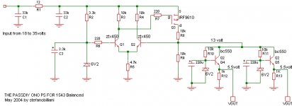
Thanks for sharing your shematic for the PS.
I am planning to build the balanced DAC with 8 pcs tda1543 for the + and 8 pcs tda1543 for the -. I will use the passive output stage for my dac to make it simple. For the PS, I have not yet decided. I think I will try using the xor ic for splitting the I2S. In the meantime, awaiting the good news from you about the dac.
Regards
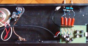
Now a fantastically bad picture of my dac (the bad picture covers some not elegant bi-used resistors) 😉
from the right there are the connector for the I2S signals , the 2 TDA1543 and then ... 2 sub regulators and the 4 D1 I/V stages.
4 philips 4.7uF MKT caps are used for the output.
The red/white shielded cable carries the +/- 30volts for the I/V and comes from outside the box since I have yet to find a small transformer for that purpose.
The inside toroid feeds the 1543s via the power supply schematic posted above .
The PS circuit is covered by the chassis. 😎
Attachments
The audio filter is a 11nF across the + and - output . I prefer it over the -cap to ground- option , ...sonically.
Here is the link where the PS schematic comes from:
http://www.passdiy.com/images/projects/pearlfig3.gif
Here is the link where the PS schematic comes from:
http://www.passdiy.com/images/projects/pearlfig3.gif
Hi stefanobilliani,
Im thinking of building this as I have all the parts on hand and would like to try a balanced dac. Would a cs8414 work here as the decoder?
Im thinking of building this as I have all the parts on hand and would like to try a balanced dac. Would a cs8414 work here as the decoder?
thanks Stefano,
I thought the cs8412 will only put an i2s signal out for dacs, what other formats are there?
I just found a post on how to do it here:
http://www.diyaudio.com/forums/showthread.php?postid=184850#post184850
I thought the cs8412 will only put an i2s signal out for dacs, what other formats are there?
I just found a post on how to do it here:
http://www.diyaudio.com/forums/showthread.php?postid=184850#post184850
can someone make several low level FFt shots (991hz -60dB dithered sinewave, FFt 4192 taps or larger), Im really interested how the individual DAC chips with vastly different low levels are summed in a balanced IV... thanks.
I used this diagram for my cs8414 http://www.fedde.nu/audio/images/nonoz3.gif
I fed the cs8414 outputs to the inputs from this diagram in the following order
http://www.diyaudio.com/forums/attachment.php?postid=382046&stamp=1083093676
sdata ----> Data ,Fsync ----> WS and Sck ----> BCK
Im not sure if my explanation is clear, but this is the configuration that seemed obvious to me. I dont have package for drawing diagrams.
I also used resistor for i/v as per nonozII.
All I get is hum, any thing simple I have got wrong?
thanks
- Status
- Not open for further replies.
- Home
- Source & Line
- Digital Line Level
- The Pass D1 For Tda1543