The R3 heatsink issue is messy - maybe the best option is to use a high-mounted heatsink without lower fins, which should allow it to comfortably clear the components around it.
The heatsink in my photo has already the smaller footprint you can probably find....
I can't see enough space for the FKP2s (C12, C30, C32) that are part of the Ultimate BOM...
I can't see enough space for the FKP2s (C12, C30, C32) that are part of the Ultimate BOM...
I've changed the outlines, but the pitch and the space around them are the same as before. Some space can be created for them, and I can revert to the original outlines easily - no problems.
I got the idea that C7 can be shifted to the left of the LM318 (next to pins 4 & 5), which will shorten the trace length from +Vs through C7 to -Vs of the LM318. This can be done by nudging the LM318 to the right by 2.5 mm or so, and rerouting one signal trace. Another advantage is that C6 and C11 can be brought closer.
Any comments/concerns about this?
I've changed the outlines, but the pitch and the space around them are the same as before. Some space can be created for them, and I can revert to the original outlines easily - no problems.
I suggest you to use C5/4.5 from the capacitor-wima library so you have the exact layout. 😉
Linuxguru, you certainly do know your way around this amp, and I apologize for my earler comments in the other thread.
Tom E
Tom, that is really nice. I did wonder about your original comment.
Linuxguru's posts, esp on the solidstate forum, have been very informative
and educational.
I built the MyRef from Uriah's first group buy, and it has been excellent.
Appreciate every effort to improve it, from everyone here.
Did anyone else find the PGND connector hard to get to, or
is it just my fat fingers?
How about an optional PGND connector in the space between C2 and C3?
is it just my fat fingers?
How about an optional PGND connector in the space between C2 and C3?
Tom, that is really nice. ......
Appreciate every effort to improve it, from everyone here.
I second that!!
Did anyone else find the PGND connector hard to get to, or
is it just my fat fingers?
How about an optional PGND connector in the space between C2 and C3?
It is hard to get to - I soldered the PGND wire, so it's not a problem for me. But people who use a tag connector may find it tiresome. I'll see if I can re-route PGND to the bottom edge.
+1!I second that!!
Regarding the PGND issue, yeah, it is a very difficult location for plugging the connector. I soldered a cable, so I have the metal tab only for measurements purposes at the moment. It will be used for earthing purposes.
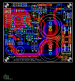
I got the idea that C7 can be shifted to the left of the LM318 (next to pins 4 & 5), which will shorten the trace length from +Vs through C7 to -Vs of the LM318. This can be done by nudging the LM318 to the right by 2.5 mm or so, and rerouting one signal trace. Another advantage is that C6 and C11 can be brought closer.
OK, I made this change and everything fell in place smoothly. Well, almost everything - C7 and C10 still need to be cleaned up a bit, which should not be a problem. The big gain was that C6, C11, the zeners and the small-signal star ground are now in a near-optimal placement and routing configuration. A side benefit is that R39, R43 and C34 could also be shifted a bit to the right, gaining additional clearance for R3 and its heatsink. C12, C30 and C32 now have the correct outline for the fat FKP2 package - a tight squeeze in some places, but managed.
Edit: Ignore the unconnected capacitor outline at the bottom - I was going to use it for C17 and C18, but left it for later.
Attachments
Last edited:
Capacitors around the opamp are really well placed now, the shortest traces are achieved.
What are you planning to stuff in R7, a miniature nuclear reactor for supplying the power IC? 😀 Now seriously, why such a really big resistor there?
What are you planning to stuff in R7, a miniature nuclear reactor for supplying the power IC? 😀 Now seriously, why such a really big resistor there?
What are you planning to stuff in R7, a miniature nuclear reactor for supplying the power IC? 😀 Now seriously, why such a really big resistor there?
Lol - a 2W Kiwame/KOA-Speer carbon-film (green), famously reputed to be lush and warm-sounding when used as the feedback resistor.
Actually, the outline I used is oversized, but the space there is not really usable for anything else, so I went with the largest package that would fit. I'll revert back to a smaller size if there's any issue with finding space for C10.
I agree, a 12k resistor will never need that size. But a nuclear reactor would be just the thing!
Just that you will have larger leads if you place a small resistor, but anyway this lenght would be made of board trace so...
Very short offtopic, is the same Kiwame than KOA-Speer?
Very short offtopic, is the same Kiwame than KOA-Speer?
Uriah, I would think that nuclear reactor should have a very low impedance. They may produce some HF ripple because all that neutrons and that stuff, but nothing that a film wima bypassing cannot filter 😉
Regards,
Regi
Regards,
Regi
Very short offtopic, is the same Kiwame than KOA-Speer?
Yes, the Kiwame is identical to the 2W KOA-Speer SPR2; it is a rebranded SPR2. KOA-Speer is also available in 1W, 0.5W and 1/4W series, but AFAIK those are not available as Kiwame.
I would like to see the PSU Zero Volts separated from the main Audio Star Ground.
The PSU zero volts carries the charging pulses between the rectifier and the first stage main smoothing caps.
If the two cap zero volt traces are taken on the bottom side direct to the Power Ground pad and spade.
That tight pair of loops carries the pulsing.
The Power Ground pad (on the bottom) coincides with the Audio Ground pad (on the top side) using the via (PTH) to the top side audio traces.
This is a very effective way of keeping charging currents out of the audio path and yet linking them with a 1.6mm long connection consisting of a solid core plug of copper wire and solder and copper plating.
Do not connect the two spade pads to the Audio Ground.
If power comes in via the spade then the power travels to and fro in the bottom side traces.
If power comes in via the hole using a soldered wire connection then the cable should better enter from the bottom.
I would like to see the PSU Zero Volts separated from the main Audio Star Ground.
Thanks, got the idea and it's easy to implement - I'll make the necessary changes. I'd also have to isolate the main PSU capacitor terminals from the audio star ground and ensure that it connects only through the large through-hole, right?
It can even be implemented on the v1.3 PCB.
Cut the cap ground traces on the top side and hardwire the cap ground pins to the wire incomer on the bottom side.
There are two Zero Volts cap pins.
Both must be disconnected from the Audio Ground on the top side.
Both Zero Volts cap pins must be connected directly to the big PTH and to the two spade pins on the bottom side.
The two spade pins must have isolated pads on the top side.
Cut the cap ground traces on the top side and hardwire the cap ground pins to the wire incomer on the bottom side.
I don't understand your rephrasing of the Zero Volts connection.I'd also have to isolate the main PSU capacitor terminals from the audio star ground and ensure that it connects only through the large through-hole,
There are two Zero Volts cap pins.
Both must be disconnected from the Audio Ground on the top side.
Both Zero Volts cap pins must be connected directly to the big PTH and to the two spade pins on the bottom side.
The two spade pins must have isolated pads on the top side.
Last edited:
There are two zero Volts cap pins.
Both must be disconnected from the Audio Ground on the top side.
Both Zero Volts cap pins must be connected directly to the big PTH and to the two spade pins on the bottom side.
The two spade pins must have isolated pads on the top side.
OK, exactly as I understood it - no problems.
- Home
- Amplifiers
- Chip Amps
- The new "My Ref" Rev C thread