What's the size of the pcbs? I don't know if your ruler is marked in mm or inches. Have you decided if you'll be selling them?
Thanks.
Regards,
Paulo.
Thanks.
Regards,
Paulo.
Last edited:
What's the size of the pcbs? I don't know if your ruler is marked in mm or inches. Have you decided if you'll be selling them?
Thanks.
Regards,
Paulo.
PB250= 3"X10" = 76 X 254 mm
PB60= 3"X 5.5" = 76 X 140 mm
ALL Voltage boards = 3" X 4 " = 76 X 102 mm
IF there is enough interest , I will sell these.
OS
PB250= 3"X10" = 76 X 254 mm
PB60= 3"X 5.5" = 76 X 140 mm
ALL Voltage boards = 3" X 4 " = 76 X 102 mm
Thank you.
That would be nice! 🙂IF there is enough interest , I will sell these.
One other thing: The KSA1381 and KSC3503 transistors are a bit difficult to source, could it be used mje340/350 in replacement?
Thanks
Regards,
Paulo.
Thank you.
That would be nice! 🙂
One other thing: The KSA1381 and KSC3503 transistors are a bit difficult to source, could it be used mje340/350 in replacement?
Thanks
Regards,
Paulo.
I had simulated Supersym I, KSA1381 and KSC3503 are critical to maintaining good performance...
Good work OS, this amp was very fast !
I had simulated Supersym I, KSA1381 and KSC3503 are critical to maintaining good performance...
That's what I suspected... I also runned some simulations with different transistors.
Where to source them?
That's what I suspected... I also runned some simulations with different transistors.
Where to source them?
They are from Fairchild, can be purchased at Digikey enjoy and buy also the TRs of output NJW1302/3281, good price!!
Where? Do they have an online shop?I sourced 2sa1381/c3503 in the UK at reasonable price.
[QUOTEhey are from Fairchild, can be purchased at Digikey ][/QUOTE]
Digikey ships from the US wich means customs wich means tax and delay...
Digikey ships from the US wich means customs wich means tax and delay...
2SA1360/2SC3423 should do it perfectly provided you stay
a little below their max VCE , i.e, 150V.
a little below their max VCE , i.e, 150V.
OK , after pulling out hair.. 
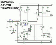
 The AX1.1VB is nearly finished. You can print it out..
A really nice "blameless" based amp , phenomenal sub .002% THD20 at 1/2 throttle (65-70W) and .0005% @ 1KHZ. I got there by NOT referencing the 2 CCS's to the "isolated ground" (PCB also has these changes). I also changed ALL small signal devices to KSA992/KSC1845 (ECB). ALL these devices are oriented for "face to face" thermal coupling.
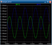
Another factor in the exceptional performance of the AX is the LTP's "CCS ADJ." I adjusted it until my LTP currents were within 10uA !! (below) 500 HZ was not as good as 10KHZ (3uA) but still pretty tight. 🙂
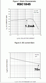
The KSC's "sweet spot" seems to be at 1.2 - 1.3mA with this amp , making for the best THD figures. BTW , the datasheet shows the highest gain and lowest Cob @ 70V / 1.2 - 1.5mA (below).
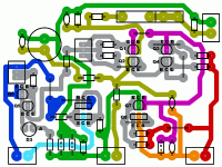
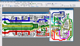
The board overview is below as well as the new schematic. Please look for any semiconductor errors (they are marked). Power lines and grounding were hopefully optimized.
Green= ground (both "dirty" and "clean" after D1/D2).
Red= V+
Orange=positive drive to power board.
Blue= V-
Light Blue=negative drive to power board.
Pink=drive to the EF VAS
Yellow = both the input and NFB signal path(s) .
OS
The AX1.1VB is nearly finished. You can print it out..A really nice "blameless" based amp , phenomenal sub .002% THD20 at 1/2 throttle (65-70W) and .0005% @ 1KHZ. I got there by NOT referencing the 2 CCS's to the "isolated ground" (PCB also has these changes). I also changed ALL small signal devices to KSA992/KSC1845 (ECB). ALL these devices are oriented for "face to face" thermal coupling.
Another factor in the exceptional performance of the AX is the LTP's "CCS ADJ." I adjusted it until my LTP currents were within 10uA !! (below) 500 HZ was not as good as 10KHZ (3uA) but still pretty tight. 🙂
The KSC's "sweet spot" seems to be at 1.2 - 1.3mA with this amp , making for the best THD figures. BTW , the datasheet shows the highest gain and lowest Cob @ 70V / 1.2 - 1.5mA (below).
The board overview is below as well as the new schematic. Please look for any semiconductor errors (they are marked). Power lines and grounding were hopefully optimized.
Green= ground (both "dirty" and "clean" after D1/D2).
Red= V+
Orange=positive drive to power board.
Blue= V-
Light Blue=negative drive to power board.
Pink=drive to the EF VAS
Yellow = both the input and NFB signal path(s) .
OS
Attachments
Great you posted that, I had a idea for a new type vas 2 3 years back which involves folded cascode but as I was very busy building 2 engines at the time I totally forgot about it and never even simmed it to have a look if its any linear. Compact folded cascode has just reminded me of the ideaTime to play a little with ltspice again 😀
Os I simmed the sym amp, but the one using Jfets, by changing to 2sk170 jfets and making 3 resistor changes the result is a amp that measures just as good as the BJT version with the advantage of higher speed. With Jfets dont use degeneration, their gm is very low, drop the degeneration resistors to 10 ohm, raise the ltp current to 2ma at least through the jfets and use 2sk170 fet, and youll get much better performance from it. THD drops from your 0.3 level to 0.004 which brings it in line with the Bjt model. If you use better jfets the performance is even better, you can also ease on the compensation as I found it to be a bit overcompensated which would improve things further.
please share... What changes ?? I will make the CX1.2FETVB out of it..
OS
there's one of my questions answered.phenomenal sub .002% THD20 at 1/2 throttle (65-70W) and .0005% @ 1KHZ. I got there by NOT referencing the 2 CCS's to the "isolated ground"
Now where is the best place to reference a cascode on the input? Signal Ground or Audio Ground (needing a separate lead out) or Power Ground?
Now where is the best place to reference a cascode on the input? Signal Ground or Audio Ground (needing a separate lead out) or Power Ground?
If my simulator are to be trusted, input cascode should be referenced to emmiter (source) resistors-> LTP CCS junction, gives the best THD.

there's one of my questions answered.
Now where is the best place to reference a cascode on the input? Signal Ground or Audio Ground (needing a separate lead out) or Power Ground?
Referencing the cascode on the CX was simple. 2 ways to do it. #1 - resistive divider between rails with a simple decoupling cap between the cascode reference and one of the rails. #2 - OR with a zener/resistor or 2 resistors (divider) between LTP "tails" and the positive rail. Both ways work very well (lowest THD/PSRR). Going directly between the rails tends to cancel out the ripple the best. Pioneer , harmon-kardon, many others use this method to create the reference... so I just had to see. Added out of phase ripple (up to 4 v p/p ) to a simulation with 75v rails. This is the way with the CX.
OS
Hey Ostripper, have you seen the CCS, and if so what do you think?
It's not secret, actually. At least I doubt it. I think Homemodder replied to one of my posts with it attached, long ago.
- keantoken
It's not secret, actually. At least I doubt it. I think Homemodder replied to one of my posts with it attached, long ago.
- keantoken
Hey Ostripper, have you seen the CCS, and if so what do you think?
It's not secret, actually. At least I doubt it. I think Homemodder replied to one of my posts with it attached, long ago.
- keantoken
I'm going to try that VoOdOo CCS on the FX , next board...
Anybody that downloaded the AX board (15 DL's), it is not faulty electrically ..BUT , I messed up 😱 😱 ... the spacing on the interface w/the powerboard .. re-download - all fixed , even nicer layout (below).
OS
Attachments
- Home
- Amplifiers
- Solid State
- The MONGREL (supersym II)