Hopefully the click bait is worthy enough.
Grab your arm chair and start screaming at the screen.
How Dare You Use the Forbidden Topology !!!
.
Reading some articles from some known Guru
Claims the (CFP) Complementary Feedback Pair Output Stage with Gain
Should be Avoided. Expect to Experience =
High Frequency Unstable
Thermally Unstable
High Distortion
Open loop Disaster
Worse yet, to get eyes to roll more. Toss in a OpAmp to drive it.
And you have what many considered some sort of abomination.
Never to have audiophile appreciation or acceptance.
Just arm wrestle the Devil for eternity
Well I ignored most the advice.
Decided to play with this Topology anyways.
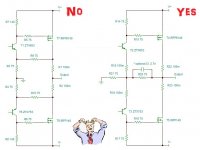
So using a typical fancy OpAmp and a CFP stage with gain.
Very Small gain, Basically a gain of 2.
I can get rid of the typical voltage swing losses you get from
Mosfets. And get pretty close as possible to Rail to Rail swing
from a 36 volt regulated power supply. or +/_ 18 volts.
Without CFP gain. I dont think it goes much more than 28 volts pp
With Gain, almost to the Rails 34.6 volts pp
* edit ( schematic updated in OP and posted in #26)
older OP garbage still in attachments
So much for the Myths of using Opamps and CFP with Gain.
Driven to Clipping its pretty close to rail to rail @ 34.65 volts
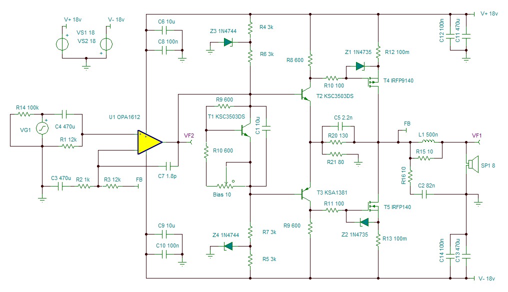
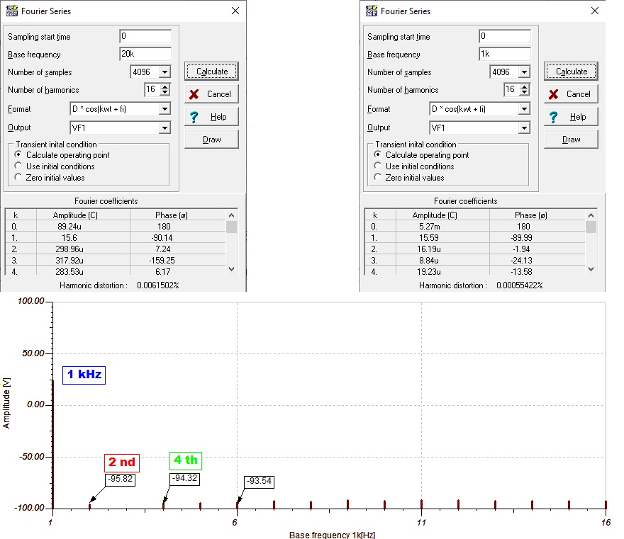
At full clean power @ 8 ohms Distortion is pretty good
@ 1 kHz .0005 %
@ 20 kHz .006 %
There you go.
2nd and 4th are high. Im sure you cant hear them @ -95 dB
really " horrible " topology
Having some Horn Loaded speaker projects coming up.
I needed something clean for 3 or 5 watts.
This gets up so close to the rails, should be good for 20/30 watts
Did I mention .0005 % distortion @ 1 kHz ?
Grab your arm chair and start screaming at the screen.
How Dare You Use the Forbidden Topology !!!
.
Reading some articles from some known Guru
Claims the (CFP) Complementary Feedback Pair Output Stage with Gain
Should be Avoided. Expect to Experience =
High Frequency Unstable
Thermally Unstable
High Distortion
Open loop Disaster
Worse yet, to get eyes to roll more. Toss in a OpAmp to drive it.
And you have what many considered some sort of abomination.
Never to have audiophile appreciation or acceptance.
Just arm wrestle the Devil for eternity
Well I ignored most the advice.
Decided to play with this Topology anyways.
So using a typical fancy OpAmp and a CFP stage with gain.
Very Small gain, Basically a gain of 2.
I can get rid of the typical voltage swing losses you get from
Mosfets. And get pretty close as possible to Rail to Rail swing
from a 36 volt regulated power supply. or +/_ 18 volts.
Without CFP gain. I dont think it goes much more than 28 volts pp
With Gain, almost to the Rails 34.6 volts pp
* edit ( schematic updated in OP and posted in #26)
older OP garbage still in attachments
So much for the Myths of using Opamps and CFP with Gain.
Driven to Clipping its pretty close to rail to rail @ 34.65 volts
At full clean power @ 8 ohms Distortion is pretty good
@ 1 kHz .0005 %
@ 20 kHz .006 %
There you go.
2nd and 4th are high. Im sure you cant hear them @ -95 dB
really " horrible " topology
Having some Horn Loaded speaker projects coming up.
I needed something clean for 3 or 5 watts.
This gets up so close to the rails, should be good for 20/30 watts
Did I mention .0005 % distortion @ 1 kHz ?
Attachments
Last edited:
The design is just for 20 to 30 watts
With regulated +/- 18 volts.
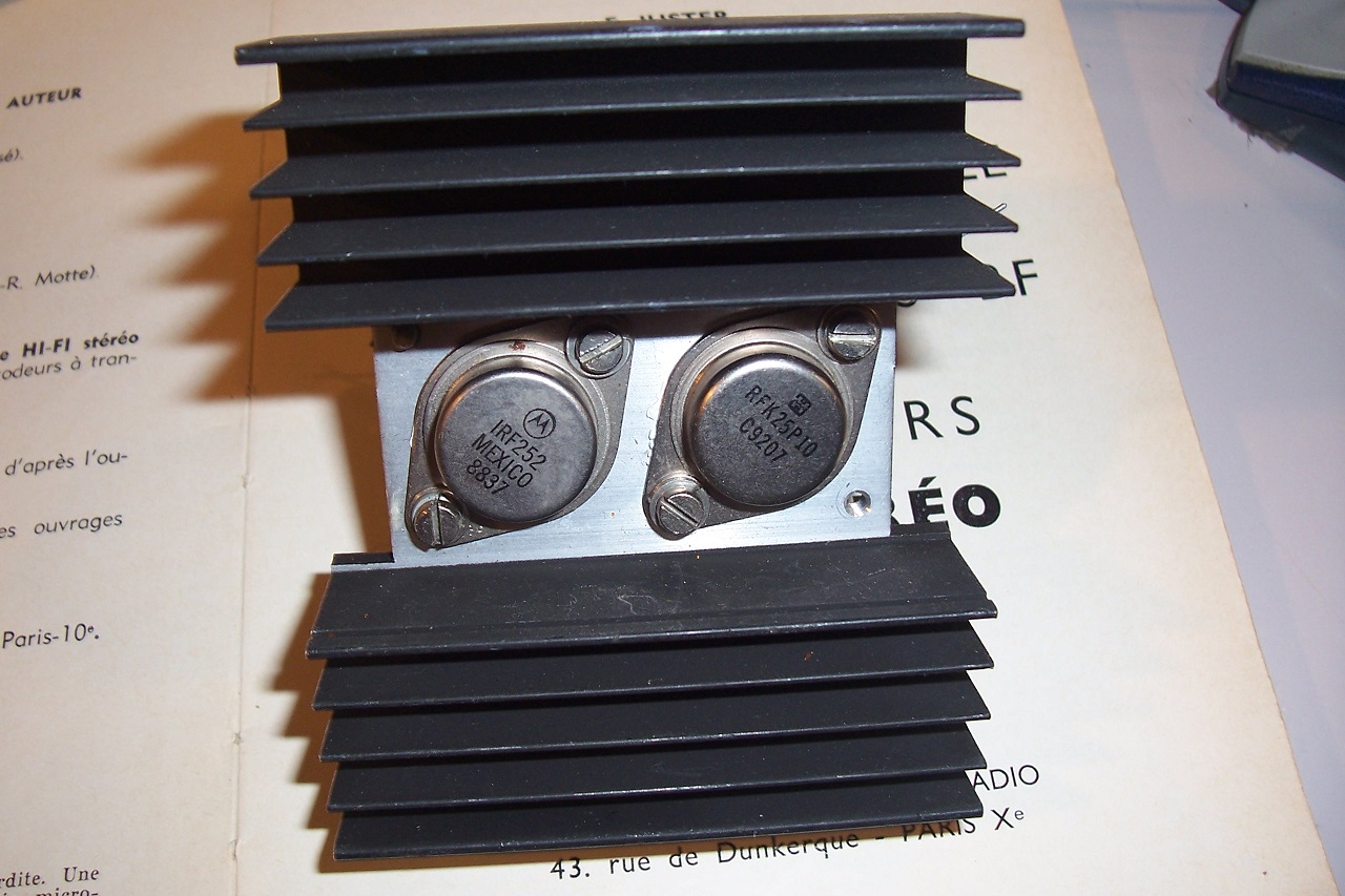
Luckily I can vary temperature of each individual stage
to detect thermal issues. With realistic approach of what real world
temp differences would be of thermal tracking.
With BJT outputs I have used additional seperate thermal tracking of the ouputs as well.
With Mosfets it doesnt seem to be as much a issue.
Of course the main concern is thermal tracking of the driver transistors
Because of the case I assumed the actual thermal differences of the T0-92 devices
would be about 20 to 25c
Assuming if the drivers dies were operating at say 45c
after that heat transfers from die to case to case to die.
thermal tracking die might only be 20 to 25c
So ive tested bias tracking of the drivers from 20 to 75c
Planned to thermally bond the current mirrors, possible with copper bands.
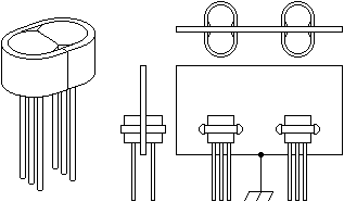
Far as the drivers and VBE. I always wanted to try to bond all 3 transistors
using a method from a 70's CFP amplifier called the gemini.
All 3 transistors mounted between 2 copper plates.
Or just track one driver mounted back to back, as shown above with copper band

With regulated +/- 18 volts.
Luckily I can vary temperature of each individual stage
to detect thermal issues. With realistic approach of what real world
temp differences would be of thermal tracking.
With BJT outputs I have used additional seperate thermal tracking of the ouputs as well.
With Mosfets it doesnt seem to be as much a issue.
Of course the main concern is thermal tracking of the driver transistors
Because of the case I assumed the actual thermal differences of the T0-92 devices
would be about 20 to 25c
Assuming if the drivers dies were operating at say 45c
after that heat transfers from die to case to case to die.
thermal tracking die might only be 20 to 25c
So ive tested bias tracking of the drivers from 20 to 75c
Planned to thermally bond the current mirrors, possible with copper bands.
Far as the drivers and VBE. I always wanted to try to bond all 3 transistors
using a method from a 70's CFP amplifier called the gemini.
All 3 transistors mounted between 2 copper plates.
Or just track one driver mounted back to back, as shown above with copper band
Attachments

Last edited:
"Nobody told me it was impossible so I just went ahead and did it".
I like heretical designs. I also noted you mercifully didn't name the guru(s) who said it cannot work.
I am also often amazed by people saying something cannot be done while the evidence is staring them in the face.
But it ain't done until you put it in hardware. Subscribing to the thread.
Jan
I like heretical designs. I also noted you mercifully didn't name the guru(s) who said it cannot work.
I am also often amazed by people saying something cannot be done while the evidence is staring them in the face.
But it ain't done until you put it in hardware. Subscribing to the thread.
Jan
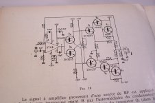
CFP with gain
Elektor did a CFA , using a CFP with gain and the "magic" C. Something quite similar, it was published almost 20 years ago.
Compact Power Amplifier from Elektor
Elektor did a CFA , using a CFP with gain and the "magic" C. Something quite similar, it was published almost 20 years ago.
Compact Power Amplifier from Elektor
suggestions
Some good ideas but:
1.R20 and R21 are unnecessarily low resistance which means they will run very hot. 75 Ohm gate resistors requires 50mA+ to drive VMOSFETs, much more than is useful.
2. 0.1 Ohm resistors are only useful in the source; of no value in the drain circuits.
3. The driver DC bias need only a tiny current with the AC drive coming from the op-amp.
4. More CFP gain allows more output voltage/power.
Attachments
The correct question is : "Why ?"
I really like people who take different paths, but I also want to understand why.
and if the answer is: "why not" that's fine with me too, but do you have a kill switch on your worktable?
Mainly taking 2 methods considered to have poor performance
and make them perform well.
I like higher powered amplifiers. But just wanted a 20 to 30 watt amplifier
only needing about 1 to 10 watts.
Simple regulated 18 volt rails so, rather small cheap capacitors
regulators etc etc. Actually just a bench power supply will run this guy
to full power.
Driving a output stage directly with a opamp has drawbacks.
Of course a opamp cant swing fully to the rails.
And mosfets can have a 3 to 4 volt loss as well. So with numerous ways to get around that.
I thought it was almost comical adding 2 resistors to a CFP stage. Instantly solves the opamp and mosfet problem and gets you fairly close to Rail to Rail. With just 2 resistors
Of course cheating a little with a fancy opamps, and using relatively fast mosfets. I was hoping for low THD.
Maybe something different, which people seem to enjoy.
Or people enjoy watching others do silly crazy things. So the overall entertainment value could play out.
Or likewise, sometimes the obvious is not obvious,
and if anybody has suggestions to make it not blow up, or address the thermal problems this
topology is known for.
The distortion and stability issues likely solved.
The whole arm wrestle with the devil is still there thermally
Some good ideas but:
1.R20 and R21 are unnecessarily low resistance which means they will run very hot. 75 Ohm gate resistors requires 50mA+ to drive VMOSFETs, much more than is useful.
2. 0.1 Ohm resistors are only useful in the source; of no value in the drain circuits.
3. The driver DC bias need only a tiny current with the AC drive coming from the op-amp.
4. More CFP gain allows more output voltage/power.
If I remember low values for r20, r21 helped reduce distortion.
But yes exactly, run hot. around 3 watts. I was thinking 5 watt resistors.
But exactly as suggested would just be better if they didnt get hot.
I will try and play around with everything suggested.
All straight forward and makes good sense.
Posting the schematic was very helpful.
I tried doing something earlier today with transistors as diodes
so was interesting to see your layout.
wow just literally noticed I put the .1 resistors on the drains in all the schematics
I posted. Little backwards from being use to Darlington's lol.
Yes exactly more gain and you can drive even higher voltage.
I noticed higher gains with the CFP is where stability gets dodgy.
So in this case just working with the limits of the opamp voltage.
Basically just a small amount of gain is all that is needed to overcome
the losses from the mosfets. And you can get a full swing to the rail.
Last edited:
Elektor did a CFA , using a CFP with gain and the "magic" C. Something quite similar, it was published almost 20 years ago.
Compact Power Amplifier from Elektor
Yes very nice
Interesting thing about CFP with mosfet or bjt
you can just use 2 zeners to protect from saturation/ overvolt
and it works out as current limit/ short circuit protection as well.
Which seems like what they have done.
Was always confused since I have seen a few designs which
suggest thermal tracking the drivers and output transistors.
like the elector design
when normally you just track the drivers.
Is this the secret to thermal stability? or would it be better
to just thermal track the drivers.
As with my design, instead of more components for the first gain stages
or differential input. Its all done with the opamp.
Its not like Im to lazy to do so. Its a matter of extreme simplicity
but very possible high performance by cheating using a
good opamp.
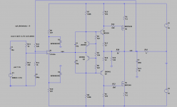
The topology has been around for a long, long time.
Here is such an early example, with opamp and everything:
Of course, in the seventies there was no question of usng MOSFETS.
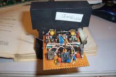
I have myself experimented with it, and had mixed results.
Here is one of my (~failed) prototype:
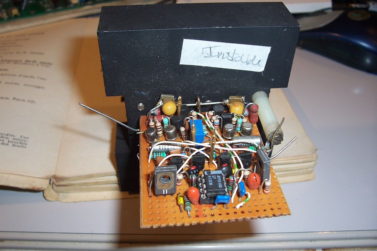
I had aimed at an insane bandwidth, and as a result the thing was not very stable.
But it's like anything: with good engineering, it is certainly possible to make it work.
Here is such an early example, with opamp and everything:
Of course, in the seventies there was no question of usng MOSFETS.
I have myself experimented with it, and had mixed results.
Here is one of my (~failed) prototype:
I had aimed at an insane bandwidth, and as a result the thing was not very stable.
But it's like anything: with good engineering, it is certainly possible to make it work.
Attachments


#12 ??????? ????????? ?? ???? ????????? ??????????? - ??????????? ?????
М.Васильев 03.01.2014 в 22:44М.
Стр. 41 журнала <<Радио>> № 5 за 1986 год
Last edited:

Here is an amp implementing "OS with gain" that was actually built, and works fine.
"Square Law Amp" designed by Ian Hegglun.
It took some effort to make it stable, but it's definitely do-able.
"Square Law Amp" designed by Ian Hegglun.
It took some effort to make it stable, but it's definitely do-able.
These things like to oscillate and then blow up, because cross conduction is worse than with unity gain stages. WHEN it oscillates, the result has a higher photon torpedo yield than a follower would. If you get it stable, that problem is solved, unless you try to drive it with a high enough frequency square wave that it becomes a problem. On only an 18 volt supply (with a current limit, even), you probably can’t generate enough energy to do any damage if something did happen.
The other issue is what happens when the stage is over driven. When the output transistor clips, the driver will continue to try to supply voltage and current. If this is managed, there will be no issue. Failure to manage it could result in overcurrent in the driver stage, and overvoltage at the mosfet gates. Try simming with a +/-50 volt supply, and drive it with close to +/-50 volts, and monitor the internal workings - the result will (and should) make you very nervous. With only a +/-18 supply, I doubt you could generate enough voltage to punch thru the oxide on the hexfets or overheat those ZTX’s. In amplifiers like the QSC PLX, baker clamps are used on the output darlingtons and the op-amp’s limited swing kept the driver current under control.
The other issue is what happens when the stage is over driven. When the output transistor clips, the driver will continue to try to supply voltage and current. If this is managed, there will be no issue. Failure to manage it could result in overcurrent in the driver stage, and overvoltage at the mosfet gates. Try simming with a +/-50 volt supply, and drive it with close to +/-50 volts, and monitor the internal workings - the result will (and should) make you very nervous. With only a +/-18 supply, I doubt you could generate enough voltage to punch thru the oxide on the hexfets or overheat those ZTX’s. In amplifiers like the QSC PLX, baker clamps are used on the output darlingtons and the op-amp’s limited swing kept the driver current under control.
I agree guys,
Sometimes a Sim wont show stability issues.
Having played with this topology in the past.
One of the main culprits is the Gain of the CFP
should be kept to the absolute minimum possible.
Of course if your driving 42 to 50 volt rails. The gain
has to be high enough.
But I have seen many designs with to much gain.
And even in sim the stability issue will show up, at high frequency.
Eventually in a comical sense, actual stability will be putting a few capacitors
in the right place to stabilize the amp.
But, if the gain of the CFP is way to high, your are fighting a loosing battle
with stability. Even with proper compensation circuits. The circuit
is likely to still be unstable if you are using to much gain in the CFP.
Best way to tell if the gain is too high.
Is to look at the output of the opamp
and drive the amp into clipping.
The opamp
will try to compensate for the clipping of the output stage.
Till it hits the top of its 15 volt rails.
If the gain is way way to high. You will see huge towers in the signal.
And you should minimize the CFP gain to reduce those towers to the bare minimum.
Of course the opamp will now use more signal swing under normal operation.
But it helps set the minimum gain needed of the CFP to keep the amp more stable.
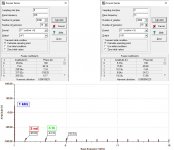
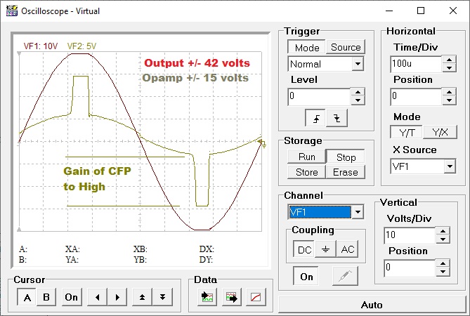
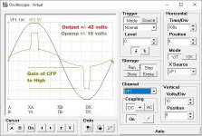
Below the scope shots show
Red output of the amplifier on a 10 volt division for a +/- 42 volts
Gold trace is set to a 5 volt Division for the opamp +/- 15 volts.
Output is driven to slight clipping and, the opamp tries to compensate.
The height of those towers shows how high the gain is set on the CFP.
So yes you are driving a amplifier to +/- 42 volts. But you are using
way way to much gain in the CFP, and it will be unstable.
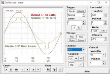
Next scope shot shows the CFP Gain significantly reduced.
But still drives output to full +/- 42 volts.
Reduce gain to bare minimum and the amplifier will
be more stable.

Sometimes a Sim wont show stability issues.
Having played with this topology in the past.
One of the main culprits is the Gain of the CFP
should be kept to the absolute minimum possible.
Of course if your driving 42 to 50 volt rails. The gain
has to be high enough.
But I have seen many designs with to much gain.
And even in sim the stability issue will show up, at high frequency.
Eventually in a comical sense, actual stability will be putting a few capacitors
in the right place to stabilize the amp.
But, if the gain of the CFP is way to high, your are fighting a loosing battle
with stability. Even with proper compensation circuits. The circuit
is likely to still be unstable if you are using to much gain in the CFP.
Best way to tell if the gain is too high.
Is to look at the output of the opamp
and drive the amp into clipping.
The opamp
will try to compensate for the clipping of the output stage.
Till it hits the top of its 15 volt rails.
If the gain is way way to high. You will see huge towers in the signal.
And you should minimize the CFP gain to reduce those towers to the bare minimum.
Of course the opamp will now use more signal swing under normal operation.
But it helps set the minimum gain needed of the CFP to keep the amp more stable.
Below the scope shots show
Red output of the amplifier on a 10 volt division for a +/- 42 volts
Gold trace is set to a 5 volt Division for the opamp +/- 15 volts.
Output is driven to slight clipping and, the opamp tries to compensate.
The height of those towers shows how high the gain is set on the CFP.
So yes you are driving a amplifier to +/- 42 volts. But you are using
way way to much gain in the CFP, and it will be unstable.
Next scope shot shows the CFP Gain significantly reduced.
But still drives output to full +/- 42 volts.
Reduce gain to bare minimum and the amplifier will
be more stable.
Attachments
The internal compensation of most op-amps depends on the output voltage so if you want the op-amp dominant pole to remain the dominant pole then the op-amp output should swing as much as possible. That should be the case for this topology but others like some Minek has done, the real VAS and therefore the dominant pole exists outside the op-amp and so the op-amp pole has to be ~cancelled, creating a huge S-curve in the phase response.
As far as the CFP stability itself, the value of the gate resistors is important. For BJT CFP, a cross coupling cap (or RC) improves XO and shoot through current but reduces PSRR.
As far as the CFP stability itself, the value of the gate resistors is important. For BJT CFP, a cross coupling cap (or RC) improves XO and shoot through current but reduces PSRR.
- Home
- Amplifiers
- Solid State
- The " Forbidden" Topology! Arm Wrestle the Devil