Due to potential for cross channel ground loop? I like the fact that the shield can be connected directly to the chassis at the point of entry.
@scottjoplin: this thread is somewhat the offspring of the discussion in the Blowtorch thread. Since the discussion has already moved on over there, I thought it wouldn't be a waste to open a dedicated thread.
It's a good idea, as you imply there is much confusion. So as not to get too carried away (yet) I believe the 3rd example is the best, close coupling of flow and returns and cross channel loop breaking resistors 🙂
Asking a shield to do two unrelated, conflicting things at once is sort of mad!
Yes, clearly.
“Input”- and “signal transfer”- related questions are also mad in SE world.
Add huge load currents dumped to the connected grounds and, of course, source<->amp HF ground loop through mains trafo parasitic capacitance.
Also, a couple questions about hot and cold impedance matching in SE->Bal connections.
Why DIY community are so conservative (not to say ortodoxal)?
Each system pretends for Hi-Q MUST have the next things:
1. Low-C sectioned El trafo through all small-signal supplies. This will allow for breaking CM-noise injection and ground-loop paths a way better than RC-breakers.
2. Symmetrical impedance-balanced signal path up to the speakers. Yes, this will double current, but takes overall high-current part from ground.
3. As short as possible high-current paths. Read as active speakers.
4. As small as possible driver-interference freq ranges. Read as 48 dB/oct filters and digital XO-ing.
5. 2-2,5 octave per driver. 4-way at least or comprehensive 3-way array of some kind. I’d prefer constant-beamwidth arc.
6. Short and slow-falling oversampling filters against brick-walls. I’d prefer to avoid digital ringing as possible.
7. Doing all of this asks for proper masterclock distribution between two digitally+active speakers. This could be done with two temperature-controlled crystals and/or relatively short speed-controlled FIFO. True bit-perfect without any ASRC.
Why there are a tons of speak about school-level designs? Why not rise our public level higher?
Nothing like testing stuff yourself.
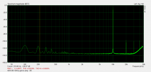
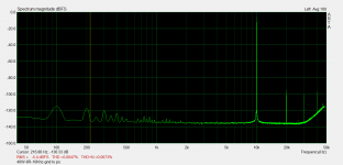
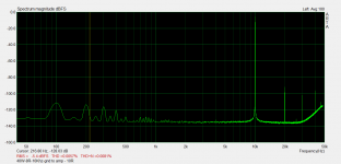
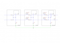
Here are three measurements made on ARTA. All are made at 10khz, 40W, 88.2khz sample rate. They are made on exactly identical amps (two channels of a lm3886 stereo amp, measuring the same normally). At 1Khz, differences were too small to measure.
The first shot is made on an amp on which the speaker return goes back to the amp pcb and without hum breaking resistor. 0.0038% thd, 0.0068% thd+n.
The second shot is made on the same amp but moving the speaker return to the PS. 0.0047% thd, 0.0073% thd+n.
The last shot is made on the second channel, which has a 10r hum breaking resistor between signal and power ground, with the speaker return going back to the amp pcb. 0.0057% thd, 0.0081% thd+n.
Attachments
Last edited:
That's opposite to what is usually found but I'm not accustomed to chip amps. They may be different.
You've done a good job of combating loops since you don't need the HBRs 🙂 or do you? have you only used it on one channel?
very contrary results to what D Joffe article says.
https://www.updatemydynaco.com/documents/GroundingProblemsRev1p4.pdf
https://www.updatemydynaco.com/documents/GroundingProblemsRev1p4.pdf
@prasi: yes and no. His article applies to a stereo amp. These measurements are in practice made on a monoblock. So I've now to see how to measure that thing on a stereo amp.
Nothing like testing stuff yourself.
Here are three measurements made on ARTA. All are made at 10khz, 40W, 88.2khz sample rate. They are made on exactly identical amps (two channels of a lm3886 stereo amp, measuring the same normally). At 1Khz, differences were too small to measure.
The first shot is made on an amp on which the speaker return goes back to the amp pcb and without hum breaking resistor. 0.0038% thd, 0.0068% thd+n.
The second shot is made on the same amp but moving the speaker return to the PS. 0.0047% thd, 0.0073% thd+n.
The last shot is made on the second channel, which has a 10r hum breaking resistor between signal and power ground, with the speaker return going back to the amp pcb. 0.0057% thd, 0.0081% thd+n.
I don't think you are performing the kind of measurement that would probe the effect of these changes to the circuit - at 40W I doubt that any hum or other interference will have a large enough contribution to change your distortion readings. So the result is not surprising to me.
What would be more revealing is a test of what is happening with no input signal (but all interconnects and speaker cables connected) to look for differences in the noise floor under the three different scenarios you mentioned.
Well, I wasn't after hum with these. I was rather trying to see the impact of where to return the speaker's return on thd and if the HBR had an impact on the performance of the amp. Some (Tomchr among others) have discouraged the use of HBRs.
So I needed heavy currents flowing through the various return and ground wires. Hence the 40W. And the impact shows mostly at higher frequencies, so 10Khz.
At this point (but it needs further testing), it looks like the use of HBR might be an exercise in balance: a bit more thd at HF but less susceptibility to ground loops. The value of the HBR is worth investigating too. I'm a bit surprised at Mark's suggestion earlier on; it seems a bit low when most places suggest 4.7r or 10r.
In that case your results are as I would expect, I'm interested to see the change with two channels, all else being kept the same for the time being
Tom is not wrong. HBR will increase THD. There are also many Diy builds where the builder spends months combating a loud and consistent hum from their amp. Solutions like disconnecting one of the interconnect shields, transformers and cutting PCB traces. After a while, you will be so desperate that THD is secondary and you will do anything for the sound of silence.
The 1ohm HBR is not new. It is also used in the My_ref amps. The two resistors are in series in the ground loop formed by the input cables/source.
The 1ohm HBR is not new. It is also used in the My_ref amps. The two resistors are in series in the ground loop formed by the input cables/source.
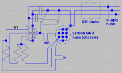
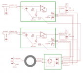
See drawing below how I layout and wire simple multi-channel (chip-)amps, eg for active speakers, when all inputs are fed from the same unbalanced source multi-channel DAC. All the input cables are tightly bundled together to minimize loop area, no pickup of external hum fields that would force ring currents along any two cable shields where the I*R drop then could cause an error signal.
The unbalanced connections automatically leads to a scheme were input and load reference must be at the exact same location with no other shared currents for lowest possible errors. And for EMC considerations this reference should be the metal chassis in the connector area which could be backed up with a piece of copper/alu sheet metal for lowest resistance and inductance, in fact a fat GND buss bar. The two signal GND connections to the amp core (input bias resistor GND and feedback network GND) are separated from the input shield connection to the buss to avoid errors from shared currents.
Not immediately clear from the drawing is the layout of the small signal components and wiring so that there is minimal area of receiving loops (an excellent testing tool for immunity here and elsewere is a tape head demagnetizer) and the high impedance traces are short or shielded for low capacitive pickup as well.
Right at the amp chip there is a rail-to-rail cap for stability, plus local bypasses, their center point also is the return of zobel/boucherot cell. After that point the local "power GND" has a path to the GND buss which is considerably higher Z than the buss bar. This is alse the return of the speaker current to the local bypasses for mid/high frequencies.
The supply bus is decoupled with a common-mode-choke which forces the net current through the choke to zero which confines recharge currents in that area. Note that the supply loop area for spiky recharge currents is minimal, for low coupling into signal lines (including the output).
The output return loop is larger (but still designed to be compact in absolute terms in order for stability into capacitive loads) and will emit a bit of audio-frequencies magnetically but since this current is very signal-correlated there is little harm done when some microscopic amount of this field might find a way back into the amp. The section of the loop which is prone of receiving fields itself is made as short as possible (amp output to GND buss) because it is outside of the feedback loop. Not shown is a L//R-cell in the ouput "hot" to prevent RF entering the amp from the speaker line.
Interconnect cable shield balancing current from the source directly enters the GND buss and will find a way to the AC-line only through the CM chokes which helps reduce it for higher frequencies. The supply itself is floating with respect to PE, that is, necessarily a class-II supply (preferably with low mains coupling by winding design), and the metal chassis is floating as well so there is little balancing current to mains line to begin with.
If one wants to use class-I supply where all its metal surroundings must be bonded to PE and the secondaries also must have path to PE than can stand fault current long enough to trip a panel breaker then the supply needs a separate PE'd metal enclosure to fulfil class-I requirements and a RCD isolator from its 0V-output to PE. But the main chassis and GND still is *not* bonded to PE directly, rather the balancing current PE path is through the chokes and the RCD. This is a form of functional earthing as opposed to safety earthing. Balancing current now has a rather low-Z direct path to PE (at audio frequencies) and this might cause I*R drops in the interconnect shields when the source has a low impedance wrt PE and the PE potentials differ. There is no way to avoid this other than with a true floating supply and chassis. Further, cross balancing current between different sources can arise even when the sink (amp) is fully floating, this can be mitigated by using complete mono-block construction where every channel has its own shielded (and preferably floating) enclosure.
Unbalanced interconnects make life hard as we must strive for zero balancing current on the shields, this is of paramount importance.
Balanced inputs looks easier for obvious reasons but the devil is in the details, especially when connected to unbalanced outputs.
Attachments
Last edited:
NEither of the schematics proposed at the start of the thread epresent a real world situation because an amplifier does not reproduce music when it's inputs are not connected to anything.
In ALL of the examples, there is a ground loop and a particularly nasty one because it happens only once the inputs are connected to the source, where in 99.99% of all cases, the grounds of the left and right channel are connected together.
It is easy to see if one draws a wire between the ground of the two channels and simply traces around from one input ground around the wiring out the other. Braiding power supply wires will do noting for this one, and it will pick up EMI from anything inside the loop, which might, for instance, be the power transformer.
Regarding the earth connector - do not EVER connect the ground to earth directly unless you are sure it is done ONLY on one of your interconnected components. Otherwise part of the return current in the various grounds will flow through loops created out of the ground connections of your components to earth and then to a common earth on the power strip where you have connected all the power cords of your components together (earth line included). I would consider an earth loop breaker mandatory.
Also, do not shield your components connecting the case to the earth wire! You are not building a stove or washing machine. If you do that, it will capacitively interact with everything in the box, via the voltage difference between the neutral mains wire and earth - pretty much any electrical disturbance or load in the building and possibly more.
The case should be connected to the component's ground and then that should go to earth via an earth loop breaker.
The case should be connected to the component's ground and then that should go to earth via an earth loop breaker.
That's not safe, the chassis must be connected directly to protective earth (unless it's Class2, double insulated)
I tend to agree with Scott here. Direct connection of earth to chassis is maybe sub-optimal but that's part of what we've got to live with (as well as unbalanced inputs and so on).
This being said, I've had a look at most of the Pass Aleph amps and they all put a thermistor between earth and chassis. :/
This being said, I've had a look at most of the Pass Aleph amps and they all put a thermistor between earth and chassis. :/
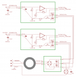
Two other schemes. One is based on Cordell's book. Speakers return to PS, zobel at input/output.
The second is hifisonix's. Speakers return to amps pcb, ground loop breaker.
If I understood Mark correctly (a caveat for all schemes btw, correct me if I've misrepresented someone's position), it would be close to his, but with 1R HBR (+ diodes across the HBR) and a resistor in // with the groundloop breaker ?
Edit: I explicitly added the input rf filter to the amps this time.
Edit: we're missing AndrewT on this thread. Maybe would I have finally been able to put into a schematic exactly what he meant with his MAG. 🙁
Attachments
Last edited:
- Status
- Not open for further replies.
- Home
- Amplifiers
- Solid State
- The dozens schemes to wire an amp...