Hi, i didn't find anywhere info about placing some text or simply components view on the top of pcb. How you do this?
Screenprinting is a traditional method. It's hard to recommend for a one-off or even a dozen boards; you have to print out the artwork as a transparency, apply photoresist to the screen, let it dry, expose it, develop it, add ink and do a few test prints to get it even, and print to your board(s). Then, assuming you're going to to reuse the screen for different graphics, clean-up involves solvents to get the ink off, and bleach to remove the photoresist. Artist or craft stores may have basic screen printing kits. IIRC the photoresist was positive, so inkjet printing on transparency film should work (might need to overlay double or triple copies to improve contrast).
Perhaps "screens" can be made directly by laser perforating some kind of film or foil. Unless you can get time on a machine like that through work/school, I assume it would cost more than just sending the board designs out to be made.
Some kind of photosensitive ink that could be applied directly to the board would be the most efficient for one or two boards. Or maybe there's some way to make normal photoresist more visible and durable?
Alternatively, (and maybe much easier), use double-sided PC board stock and do the labels in copper. Or print onto some kind of label stock that looks OK when stuck on the board.
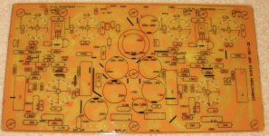
Component Ident or silk screen, if you are doing the design on a CAD system you have a seperate layer for the graphics and text that a manufacturer will use to create the artwork, not so easy for home construction.
I'm assuming home made PCBs. If you use the toner tranfer method, just print up the top silk layer reversed (flipped L to R or up to down). After etching the PCB, removing the toner and drilling, align and iron on the top and remove the paper as normal. The toner is black, but most homemade boards are white, so it works for good contrast. It's not as nice looking as silkscreen, but it works well enough.
Last edited:
Look for some peel apart clear label sheets. I had some that would work in an inkjet but turned invisible when stuck to an envelope. Kind of translucent white and very thin. Could print up parts designators or even outlines and then stick sheet to board. Only problem I see is pain of poking all them holes through overlay. Another option is find an old flatbed x-y plotter and use it to draw your lettering..... I'm done.
Doc
Doc
I remember reading that dusting talcum powder after
toner transferring the silk layer and baking it a little (or hold
a hot clothes iron as close as possible, for a few seconds)
should give you a white silk layer. Haven't tried it myself.
toner transferring the silk layer and baking it a little (or hold
a hot clothes iron as close as possible, for a few seconds)
should give you a white silk layer. Haven't tried it myself.
- Status
- Not open for further replies.
- Home
- Design & Build
- Construction Tips
- text on top of pcb