Don't forget Murphy's Law.
Post #20 adds 4 parts to the original design and guarantees startup. If its 10K pullup resistor is rated for 1 watt or more, it will operate properly with input voltages as high as 80 volts. And if you select a 2 watt resistor in this position, the circuit will work just fine with 100 volts of input.
If you are frightened that it may conduct unwanted AC signals ("noise") from the raw input pin to the current source, I suggest you simulate the circuit to see just how large or small the effect may be. {answer: small}.
However, if you want to reduce noise injection still further, you have several options
- Connect a 10uF filter capacitor in parallel with the 4.7V zener diode. This filter has a cutoff frequency is 1/(2*PI*Cfilter*2.1K) -- well below the lowest audio frequency. {10K parallel 2.7K equals 2.1K}
- Change the 1N4148 diode (4 pF) to a 1N4149 diode (2 pF), lowering the injection by 2X
- Put two 1N4149 diodes in series, lowering the injection by another 2X
- Connect another filter capacitor from the diode cathode to ground.
Gosh! I can see that if I don't post quickly I shall acquire a reputation for undue recklessness. There's no need to worry. I still stand by my earlier statement
<<<
for correct circuit operation to rely on things like having sufficient MOSFET gate drain capacitance, or transistor behavior at base emitter voltages that are only a fraction of a diode drop, seems rather reckless. So the precautionary principle applies, and the issue must be addressed.
>>>
When I wrote
<<<
I'm now thinking of building it without the startup guarantee parts at first to see if it would start anyway.
>>>
My plan was (and is) to include the startup guarantee parts in the BOM and on the layout, but not to no solder them in place when I first stuff the board. Then, if it doesn't start, it will be easy to mount them afterward.
I intend to use this regulator for a combination pre-amp and headphone amp (a sort of miniature power amp), with 2 regulators & 1 channel of amplification per board. The layout for that board will also include the startup guarantee circuitry, even if the test regulator always starts without it.
But, if the test regulator does always start without the startup guarantee circuitry, then the parts for it will also be not fitted (at least at first) on the combination pre-amp and headphone amp boards – to see if they also startup unassisted.
Who knows what will happen – knowledge of that waits on building and seeing. But it is conceivable that there could end up being 5 regulators all starting unassisted. It's what led to pondering the issue of how much empirical evidence is required to have confidence in a circuit, when a complete theoretical analysis isn't practical. Or, to put it the other way round, how much unnecessary stuff's in the world's electronics just because nobody can prove for sure that it's not needed.
P.S. Ketje's way for doing it's simpler than mine. I'll post a revised schematic soon.
<<<
for correct circuit operation to rely on things like having sufficient MOSFET gate drain capacitance, or transistor behavior at base emitter voltages that are only a fraction of a diode drop, seems rather reckless. So the precautionary principle applies, and the issue must be addressed.
>>>
When I wrote
<<<
I'm now thinking of building it without the startup guarantee parts at first to see if it would start anyway.
>>>
My plan was (and is) to include the startup guarantee parts in the BOM and on the layout, but not to no solder them in place when I first stuff the board. Then, if it doesn't start, it will be easy to mount them afterward.
I intend to use this regulator for a combination pre-amp and headphone amp (a sort of miniature power amp), with 2 regulators & 1 channel of amplification per board. The layout for that board will also include the startup guarantee circuitry, even if the test regulator always starts without it.
But, if the test regulator does always start without the startup guarantee circuitry, then the parts for it will also be not fitted (at least at first) on the combination pre-amp and headphone amp boards – to see if they also startup unassisted.
Who knows what will happen – knowledge of that waits on building and seeing. But it is conceivable that there could end up being 5 regulators all starting unassisted. It's what led to pondering the issue of how much empirical evidence is required to have confidence in a circuit, when a complete theoretical analysis isn't practical. Or, to put it the other way round, how much unnecessary stuff's in the world's electronics just because nobody can prove for sure that it's not needed.
P.S. Ketje's way for doing it's simpler than mine. I'll post a revised schematic soon.
If you send me your address I will be glad to send you a gift of all the parts needed to build ten copies of the startup circuit in post #20. These will cost me $4.37 plus postage (qty=10 pricing from Digi-Key); an amount I consider small. Rest assured, this gift will not bankrupt me.
Last edited:
It lifts my spirit that my 1st circuit posted here should generate the offer of a gift! Thank-you.
THE LAYOUT WILL UNQUESTIONABLY INCLUDE THE POST #30 STARTUP CIRCUITRY, I can also afford the parts 🙂 Indeed, other than the need to visit Radio Shack for a 5v zener, and the requirement to make higher wattage resistors from 1/4 watt ones, I already have the parts.
Having come up with this circuit there's no way I'll let it fail merely for lack of startup circuitry. I just want to try the experiment of seeing what happens without it.
My real reason for resiting adding parts is the eternal quest for simplicity in design. If I don't watch out for it, I tend to gold plate everything, including the gold plating, ad infinitum.
I think there's very little danger of noise injection through the diode junction capacitance for the following reasons.
The slew rate across 4pF required to equal Q3's collector current of about 3.5 mA is 3.5E-3/4E-12 = 875 v/us. To get 1/1000 of Q3's collector current (noise 60 dB below output) still requires almost 1 v/us. Past experience suggests that the max dv/dt at the top of the zener will be less than 1 v/us. And, once the noise has entered Q3s collector current, no less than 3 active feedback stages reduce it still further before it reaches the output. These being the complimentary feedback pair Q2 & Q3, the complimentary feedback pair X1 & Q1, and, of course, the shunt itself.
Still, it's good to be made aware of the 1N4149's factor of 2 reduction in junction capacitance over the 1N4148. Is it inferior in any way to the 1N4148? I've tended to use 1N4148s because I already have a whole bunch of them. Now I think I should get a whole lot of 1N4149s.
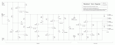
Note that since I don't already have stocks of higher wattage resistors, the attached circuit sometimes uses 1/4 watt resistors in parallel or series to make higher power resistors. It's a test circuit, subsequent versions will use normal 1/2 watt resistors, etc.
THE LAYOUT WILL UNQUESTIONABLY INCLUDE THE POST #30 STARTUP CIRCUITRY, I can also afford the parts 🙂 Indeed, other than the need to visit Radio Shack for a 5v zener, and the requirement to make higher wattage resistors from 1/4 watt ones, I already have the parts.
Having come up with this circuit there's no way I'll let it fail merely for lack of startup circuitry. I just want to try the experiment of seeing what happens without it.
My real reason for resiting adding parts is the eternal quest for simplicity in design. If I don't watch out for it, I tend to gold plate everything, including the gold plating, ad infinitum.
I think there's very little danger of noise injection through the diode junction capacitance for the following reasons.
The slew rate across 4pF required to equal Q3's collector current of about 3.5 mA is 3.5E-3/4E-12 = 875 v/us. To get 1/1000 of Q3's collector current (noise 60 dB below output) still requires almost 1 v/us. Past experience suggests that the max dv/dt at the top of the zener will be less than 1 v/us. And, once the noise has entered Q3s collector current, no less than 3 active feedback stages reduce it still further before it reaches the output. These being the complimentary feedback pair Q2 & Q3, the complimentary feedback pair X1 & Q1, and, of course, the shunt itself.
Still, it's good to be made aware of the 1N4149's factor of 2 reduction in junction capacitance over the 1N4148. Is it inferior in any way to the 1N4148? I've tended to use 1N4148s because I already have a whole bunch of them. Now I think I should get a whole lot of 1N4149s.
Note that since I don't already have stocks of higher wattage resistors, the attached circuit sometimes uses 1/4 watt resistors in parallel or series to make higher power resistors. It's a test circuit, subsequent versions will use normal 1/2 watt resistors, etc.
Attachments
I see a Racal/Dana 9302 R.F. Millivoltmeter (10kHz to 1.5GHz, 1mv RMS FSD at its most sensitive setting) here on ebay:Although I have a scope similar to yours, its a pain using it to quantify low level signals - I reckon you'll be better off investing in an AC millivoltmeter. I find mine invaluable and it was fairly inexpensive.
Racal Dana 9302 R F Millivoltmeter 1 5 GHz Guaranteed | eBay
Does anybody know if it looks like a good buy or not?
If I touch the probe to the regulator output will it simply read the RMS voltage over 10kHz to 1.5GHz?
Can you also use this type of meter to “sniff” for oscillations in a circuit by holding the probe close to different parts of the circuit in turn?
Does it have other uses?
Thanks for any info.
That one looks to be a bit wider bandwidth than you're likely to need. I suspect as a result you give up the most sensitive range - mine's 1MHz BW and goes down to 300uV.
If you like the 2.0 pF 1N4149 then you will really love the 0.3 pF 1SS427 from Toshiba, datasheet attached. 30 cents in Qty=1 at Digikey, 9.7 cents in Qty=100 at Chip One Stop (a fully authorized Toshiba distributor).
It's a surface mount device but don't let that scare you. After watching a couple of YouTube tutorials and doing 60 minutes of practice, you too will be able to solder low-pincount SMD devices by hand. That's how I learned. That's how lots of people learned. You'd need way-below-average skills and waaaay-below-average tenacity, to fail at soldering 2-pin SMDs.
With dirt-cheap PCB fabrication widely available (see post#4 in this thread), there's no reason to avoid SMD resistors, capacitors, diodes, and transistors. If you want to wait a few boards before trying your hand at SMD integrated circuits, go right ahead.
Attachments
AHA! I changed search term from “RF Millivoltmeter” to “AC Millivoltmeter” and presto! instruments with specs like Abraxalito's. I ordered a dual channel unit off of ebay for $100 + $40 shipping. 10Hz to 1MHz bandwidth, 0.3mv FSD maximum sensitivity. It says each channel has an output. Are these devices also usable as pre-amps?That one looks to be a bit wider bandwidth than you're likely to need. I suspect as a result you give up the most sensitive range - mine's 1MHz BW and goes down to 300uV.
Yep - I have one channel of my scope to the output of the voltmeter, allows viewing much smaller amplitude signals clearly.
Yep - I have one channel of my scope to the output of the voltmeter, allows viewing much smaller amplitude signals clearly.
Now that I get that it's also a (2 channel) pre-amp, I can see that this will be a generally useful addition to my test kit.
I've also discovered another interesting variation on the theme, the Philips Pm 2554 millivoltmeter. It's not as sensitive, only going down to 1mv FSD. But that's 1mv FSD with a bandwidth from 2Hz to a top end -3dB point of about 30MHz, with a pre-amp output available. Input's by an ordinary BNC connector, not a special probe like the out beyond 1GHz meters use.
It's a surface mount device but don't let that scare you. After watching a couple of YouTube tutorials and doing 60 minutes of practice, you too will be able to solder low-pincount SMD devices by hand. That's how I learned. That's how lots of people learned. You'd need way-below-average skills and waaaay-below-average tenacity, to fail at soldering 2-pin SMDs.
Yes, perhaps I've got a bit too good at procrastinating surface mount soldering. You goad me into it. Though not for this project, since it's all through hole parts. And the next one (the pre-amp/headphone amp that will use this regulator) is already designed -- also with through hole parts. But after that some SMD may come. The pool of good but SMD only parts grows by the day, as the 1SS427 illustrates.
Has anyone tried the template, solder paste & hotplate method? Can you do it on your kitchen stove in an old non-stick frying pan using a thermocouple to check the pan temperature? Are the templates or the paste ludicrously expensive?
I do worry a bit about the ease of modifying a prototype board constructed as a surface mount PCB. For example, it sure doesn't seem like it would be as easy to tenfold a capacitor's value on a surface mount prototype board as on a through hole board.
In the interim a bag of 1N4149s is on order, and I've been learning GEDA PCB layout. I've started making footprints for the components in the regulator, which must then be attached to the schematic. Then layout proper can begin.
So far, a double sided PCB with a ground plane's planned, having the 2 power MOSFETs in the regulator & the 47uF capacitor as close as possible, the rest of the regulator parts on one 1 side of them, and the test circuitry on the other side.
Electrolytics don't like high temperatures,better not too close to hot items like power mosfet's.So far, a double sided PCB with a ground plane's planned, having the 2 power MOSFETs in the regulator & the 47uF capacitor as close as possible, the rest of the regulator parts on one 1 side of them, and the test circuitry on the other side.
Mona
Has anyone tried the template, solder paste & hotplate method? Can you do it on your kitchen stove in an old non-stick frying pan using a thermocouple to check the pan temperature? Are the templates or the paste ludicrously expensive?
I have used a induction hotplate which has a temp setting and a special handled 'plate' to convert it for use with normal pans. I just place the PCB (with solder paste and parts placed) on the plate, cover with a clear Pyrex bowl and place the plate on the induction hob. You'll see the solder paste melt and it's fairly obvious when you should remove the plate and Pyrex bowl and very carefully slide the PCB off onto another (temp proof) surface for cooling.
I have printed the circuit board actual size to clear sheets of mylar and cut stencils manually with a scalpel. It works very well.
However, simply hand soldering the SMD parts is much less fuss. I have found it helpful to sometimes slightly enlarge some pads when doing the board to make the hand soldering a little easier. Give it a whirl; practice makes perfect. I'm a newbie and if I can do it anyone can.
I see your point. How much space do you think is enough?Electrolytics don't like high temperatures,better not too close to hot items like power mosfet's.
Mona
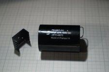
Attached is a photo of 1 of the bolt on heatsinks for the MOSFETs. If necessary, 2 can be used on the same MOSFET, mounted back to back. They came from Mouser:
Mouser Electronics - Catalog Viewer
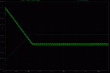
Also in the photo is the capacitor in question. It's a metalized polypropylene film type, not an electrolytic. The LTSpice plot (starting at power on) shows the no load on the regulator heat dissipation of X1 (in green) and X2 (in cyan) with a transformer secondary of 24v RMS (34 peak to peak) at 50Hz with IN4001 bridge rectifier diodes and 1mF smoothing. As you can see the numbers are actually quite small -- Ah, the luxury of specifying a low maximum output current at the outset.🙂
Attachments
I mentioned before getting a meter which also functions as an oscilloscope pre-amp. It's arrived, and I investigated it a bit to see how well it works. I've posted a little report about it here:
http://www.diyaudio.com/forums/equipment-tools/278814-little-look-cheap-ac-millivoltmeter.html
http://www.diyaudio.com/forums/equipment-tools/278814-little-look-cheap-ac-millivoltmeter.html
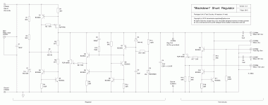
Preliminary 1st Draft PCB Layout
My life's been a little busy these last few weeks, and it's taken me some time to learn the gEDA PCB layout tool. But I can now make component footprints, and link them to schematic symbols. With these new (to me) abilities I've done my 1st PCB layout since the 1980s!
It's a preliminary 1st draft, and all suggestions, comments and criticisms are welcome.
At the very least I'll be looking again at the matter of the drill sizes. A micrometer is on order from Ebay, so that I can measure component wire diameters.
I swapped over the resistor and capacitor in the lag compensation network, so as to make it easier to change the capacitor once the PCB's stuffed. Hence the revised circuit diagram.
In the layout the test circuitry's on the left, and the regulator proper's on the right I anticipate redoing the layout when the regulator actually gets used. This layout's purely for test purposes.
Please could you post a link to this PCB source.
My life's been a little busy these last few weeks, and it's taken me some time to learn the gEDA PCB layout tool. But I can now make component footprints, and link them to schematic symbols. With these new (to me) abilities I've done my 1st PCB layout since the 1980s!
It's a preliminary 1st draft, and all suggestions, comments and criticisms are welcome.
At the very least I'll be looking again at the matter of the drill sizes. A micrometer is on order from Ebay, so that I can measure component wire diameters.
I swapped over the resistor and capacitor in the lag compensation network, so as to make it easier to change the capacitor once the PCB's stuffed. Hence the revised circuit diagram.
In the layout the test circuitry's on the left, and the regulator proper's on the right I anticipate redoing the layout when the regulator actually gets used. This layout's purely for test purposes.
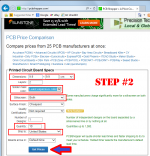
Here are today's prices for 2 layer PCBs, 4 inches by 4 inches, shipped to the United States. Notice (blue rectangle) that you get ten copies of the board.
Depending on whether you want the lowest cost, or the fastest turnaround, you can expect to pay $16 to $33 for ten boards. That's dirt cheap. Dirt the fword cheap.
Please could you post a link to this PCB source.
Attachments
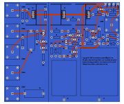


I wonder whether the values of load resistors R15 and R16 might be misprinted? The load currents look awfully small for a supply designed to deliver 80 mA; see red arrows in attachment.... preliminary 1st draft, and all suggestions, comments and criticisms are welcome. ...
_
Attachments
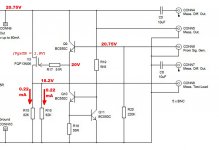
OMG. Thanks for spotting that mistake.I wonder whether the values of load resistors R15 and R16 might be misprinted? The load currents look awfully small for a supply designed to deliver 80 mA; see red arrows in attachment.
They're intended to be 82R not 82K of course. Thus in parallel making a 41R resistor, which reaches 0.5W dissipation at 110mA and 4.52v.
I think I'd have noticed when it got to soldering them on to the board. But if I didn't notice, then I could have ended up fooling myself into thinking the regulator had next to immaculate performance, when the facts would actually be failure to perform any real testing.
Attachments

PCB Hole Size Panic
I worried about the hole sizes in the PCB layout I posted earlier in this thread. They do look rather haphazardly chosen. So I got a micrometer (about $40 on eBay) and measured the lead diameters on the components to be used in the prototype. Hence I now know the sizes of the wires that will go through the holes in the PCB But 3 questions remain.
1) How much clearance space is needed between the outside of the wire passing through the hole in the PCB and the inside of the hole?
2) How much margin of error must be allowed for the PCB maker using a best-fit drill size, instead of exactly the size in the drill file?
3) Do the plated through holes in a manufactured PCB actually end up with the same diameters as the diameters given in the PCB's (excellon) drill file?
Question 3 may seem a bit strange. But what gives me pause for thought is that they're called drill sizes, and the hole does end up smaller than the diameter of the drill that bored it. That's because after drilling the inside of the hole gets plated with copper, thus reducing the radius of the hole by the thickness of the copper plating.
Any help with these questions would be most appreciated.
- Status
- Not open for further replies.
- Home
- Amplifiers
- Power Supplies
- Testing a New Design Shunt Regulator