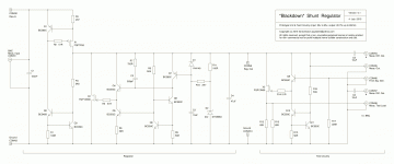
Testing Another Regulator
I've been amusing myself designing a low current (80 mA) shunt regulator. Since you guys have been discussing regulator testing, I thought I'd post what I'm planning here, and ask if it looks like a sensible plan.
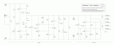
I have a Rigol DS1102E scope, and a Hantek HDG2022B signal generator (sine, square, triangle, etc.). The circuit diagram shows what I'm planning to build, on the solder breadboard in the picture. My intent is to solder BNC sockets onto the breadboard, and connect the scope with BNC cables, instead of using normal scope probes. The idea being that the loss of bandwidth is more than compensated for by not having RF hash picked up by the probe ground connection, and by the 10-fold increase in voltage sensitivity.
I'm hoping to measure regulator output impedance at half a dozen or more frequencies by setting the signal generator to make a sine wave, and scoping the sizes of the sine waves at the source of X3 (CONN8) and the regulator output (CONN5). The transient response can be examined by doing the same, with the signal generator making a square wave.
For a best effort output voltage transient response measurement the idea is to put the scope in chan1 minus chan2 mode and make a differential measurement, comparing the voltage at ground (CONN7) and the regulator’s output (CONN5). For this there'll be (1 watt) 50 ohm line terminators at the scope end of the BNC cables, and the cable shields will be connected to ground only at the scope end. The breadboard will include a couple of Panasonic polyester 10uF DC blocking capacitors (C5 & C6) in series with the differential measurement BNC connectors, to avoid overloading the regulator and prevent things from burning up.
Do you think I'll be able to make good measurements this way? Will the twisted nature of the (not yet designed) solder breadboard layout mess things up and make the effort of providing a clean scope connection redundant?
I've been amusing myself designing a low current (80 mA) shunt regulator. Since you guys have been discussing regulator testing, I thought I'd post what I'm planning here, and ask if it looks like a sensible plan.
I have a Rigol DS1102E scope, and a Hantek HDG2022B signal generator (sine, square, triangle, etc.). The circuit diagram shows what I'm planning to build, on the solder breadboard in the picture. My intent is to solder BNC sockets onto the breadboard, and connect the scope with BNC cables, instead of using normal scope probes. The idea being that the loss of bandwidth is more than compensated for by not having RF hash picked up by the probe ground connection, and by the 10-fold increase in voltage sensitivity.
I'm hoping to measure regulator output impedance at half a dozen or more frequencies by setting the signal generator to make a sine wave, and scoping the sizes of the sine waves at the source of X3 (CONN8) and the regulator output (CONN5). The transient response can be examined by doing the same, with the signal generator making a square wave.
For a best effort output voltage transient response measurement the idea is to put the scope in chan1 minus chan2 mode and make a differential measurement, comparing the voltage at ground (CONN7) and the regulator’s output (CONN5). For this there'll be (1 watt) 50 ohm line terminators at the scope end of the BNC cables, and the cable shields will be connected to ground only at the scope end. The breadboard will include a couple of Panasonic polyester 10uF DC blocking capacitors (C5 & C6) in series with the differential measurement BNC connectors, to avoid overloading the regulator and prevent things from burning up.
Do you think I'll be able to make good measurements this way? Will the twisted nature of the (not yet designed) solder breadboard layout mess things up and make the effort of providing a clean scope connection redundant?
Attachments
Although I have a scope similar to yours, its a pain using it to quantify low level signals - I reckon you'll be better off investing in an AC millivoltmeter. I find mine invaluable and it was fairly inexpensive.
Do you think I'll be able to make good measurements this way? Will the twisted nature of the (not yet designed)
solder breadboard layout mess things up and make the effort of providing a clean scope connection redundant?
It would be better to have an actual pcb with a ground plane.
Last edited:
I'm sure you can lay out that circuit on a 2 layer PCB whose dimensions are 3.9 inches by 3.9 inches, or less.
Here are today's prices for 2 layer PCBs, 4 inches by 4 inches, shipped to the United States. Notice (blue rectangle) that you get ten copies of the board.
Depending on whether you want the lowest cost, or the fastest turnaround, you can expect to pay $16 to $33 for ten boards. That's dirt cheap. Dirt the fword cheap.
_
Attachments
I'm sure you can lay out that circuit on a 2 layer PCB whose dimensions are 3.9 inches by 3.9 inches, or less.
For a few smaller pcbs, Osh Park is just great.
Last edited:

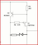
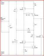
Yes it does appear that R4 is connected incorrectly, leading to a stable state with the current source "X1" completely cut off, and the output "CONN.9" at ground.A question, how does the circuit start-up ?
Mona
I recommend moving the top of R4 to "CONN.2" which guarantees startup.
If you wish, you can split R4 into two series resistors, each 2.7K, and connect a bypass capacitor to the midpoint. C>22uF puts a pole at 6 Hertz or lower, providing some 100Hz mains ripple rejection without slowing down the wakey-uppy transient too much.
Or for the same budget of 3 components you could achieve even greater mains ripple rejection by connecting the resistor midpoint to a zener diode instead of a bypass capacitor. Voila, constant ripple rejection vs frequency, all the way down to DC. Oh baby.
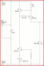
You can get rid of the potentiometer AND increase the current soure's insensitivity to supply variation, if you remove the JFET and replace it by two resistors and one zener diode. Schematic below.
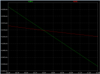
The green trace shows the JFET startup circuit. Current in PNP transistor Q1 is plotted, while the supply voltage is varied from 28V to 32V. The red trace shows the 2R+1Zener circuit. Current in PNP transistor Q2 is plotted.
As you can see, Q2 is fed a more constant current than Q1. The red trace is flatter (varies less) than the green trace. And there's no potentiometer to fiddle with.
_
Attachments
Looks like the voltage change of the zener is smaller then the Ri of the fet (still over 200k).I choose the J203 for it's Vds of max.40V, perhaps there are better ones.
The advantage is that nothing change for different voltages, with a zener you must readapt the resistance (and perhaps the zener).
Mona
The advantage is that nothing change for different voltages, with a zener you must readapt the resistance (and perhaps the zener).
Mona
And using the DIY principle "if some is good, then more is better" we observe that adding 1 more zener and 1 more resistor improves performance still further. We also observe that combining the two approaches (JFET trimmed current source, 2R+1Z bootstrap) improves performance as well.
Thanks
Thanks to Mooly for sorting out the thread mess.
And thanks to everyone who's taken an interest. This is the 1st time I've ever posted a circuit diagram here, and only my 10th posting overall. The high quality of all the responses makes the activity good fun. 🙂
Thanks to Mooly for sorting out the thread mess.
And thanks to everyone who's taken an interest. This is the 1st time I've ever posted a circuit diagram here, and only my 10th posting overall. The high quality of all the responses makes the activity good fun. 🙂
Holy Mackerel Batman!!!
It's cheaper to send the solder bread board pattern off as a custom PCB than it is to buy the thing as a mass produced in stock off the shelf item!!!
Do solder bread board makers live off of people like me who are just slow to notice how dramatically PCB prices have come down?
I haven't done a PCB layout in more than 2 decades. But I've abandoned my solder bread board plan, this weekend I shall start learning the GEDA PCB layout software that integrates with my schematic editor.
Actually, a nagging doubt had been building up in my mind about being able to get decent performance on the breadboard from before posting here. What others have said only confirms that doubt.
Stuck State
I'm still thinking about the stuck state on startup issue. I do like that none of the suggested fixes add any (big & expensive) capacitors to the circuit. The performance of MJ's zener current sink seems remarkably good for the parts used.
I'm thinking about a solution with a zener where it only conducts during startup, and leaves the circuit unchanged the rest of the time. More to come in the next few days.
I'm not sure that there are any better ones. The current selection of in production through hole JFETs is really rather miserable.
I'm still thinking about the stuck state on startup issue. I do like that none of the suggested fixes add any (big & expensive) capacitors to the circuit. The performance of MJ's zener current sink seems remarkably good for the parts used.
I'm thinking about a solution with a zener where it only conducts during startup, and leaves the circuit unchanged the rest of the time. More to come in the next few days.
I choose the J203 for it's Vds of max.40V, perhaps there are better ones.
I'm not sure that there are any better ones. The current selection of in production through hole JFETs is really rather miserable.
I'd not ditch the breadboard approach so quickly. The big advantage of the breadboard is its interactive - breadboarding is a way to learn what's critical in the layout and what isn't. So breadboarding is learning by feedback.
In contrast PCB design is feedforward - you need to know what the error sources are going to be to head them off in advance. Which is why PCB design makes sense after extensive breadboarding. Doing a PCB first means in practice it'll get converted into a breadboard soon enough....
In contrast PCB design is feedforward - you need to know what the error sources are going to be to head them off in advance. Which is why PCB design makes sense after extensive breadboarding. Doing a PCB first means in practice it'll get converted into a breadboard soon enough....
I'm thinking about a [startup circuit] with a zener where it only conducts during startup, and leaves the circuit unchanged the rest of the time. More to come in the next few days.
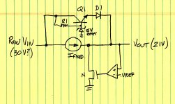
A circuit on Samuel Groner's website shows one way to do this. He's got a "Discrete Series Voltage Regulator" (LINK) that does not successfully start up until there's significant voltage across the 5.0 volt reference diode. He uses a 4.3V zener and an 0.7 volt normal 4148 silicon diode to pull the reference up to (4.3 - 0.7) = 3.6 volts. Then the regulator starts up, the VREF diode goes all the way up to 5 volts, which reverse biases the startup 4148 diode and takes it out of the circuit completely.
Figure 1 below shows one way to do the same thing with your (CCS + shunt) regulator. Power transistor Q1 and power diode D1 pull the regulator output up to 13.6 volts (Vzener - (Vbe + Vdiode)) which is enough to get the regulator started. Once the regulator goes to work, it sets the output to the desired 21V, which reverse biases D1 and removes the startup circuit completely. Thanks to Q1 this circuit can pump enormous current into the output if need be, during startup. (Maybe you've got 100,000 microfarads and yet you want to start up quickly??)
Figure 2 is a more minimalist implementation. A zener diode pulls the output up to (Vin - (Vzener + Vdiode)). If the zener voltage is 16V and if Vin is 30V then the output is pulled up to 13.3 volts or so. This is plenty high enough to wake up the regulator circuitry, so it functions correctly and eventually sets the output to 21V. That reverse-biases D2 and completely removes the startup mechanism from the final circuit. The circuit's ability to deliver enormous current to the load during startup, is limited by the current ratings of the zener diode and the series diode. Thru-hole zeners rated for 5 watts (approx 0.4 amperes) are about the biggest available.
Attachments

Gosh this startup problem's a thorny issue. Whilst it's clear that the circuit has a stuck state, it's less clear that it will ever actually enter the stuck state.
I thought about not doing anything about it at all.
To get into the stuck state when power's applied, the voltage at the gate of X1 must rise very very nearly as fast as the (slowish) rise in voltage at the regulator input, so that MOSFET X1 never conducts. Where does the current to charge X1's gate drain capacitance come from? From Q1? For this to happen it seems to imply that during power up Q1's collector emitter resistance is significantly more than 30 times less than Q2's, the more being to provide the charging current for X1's gate drain capacitance, and the 30 being Q1 and Q2 acting as a potential divider holding X1's gate voltage close enough to the input to prevent X1 from ever turning on. So far I've been unable to come up with a reason for this big a difference in collector emitter resistance between the 2 transistors.
But I also sure can't prove that it won't happen. And for correct circuit operation to rely on things like having sufficient MOSFET gate drain capacitance, or transistor behavior at base emitter voltages that are only a fraction of a diode drop, seems rather reckless. So the precautionary principle applies, and the issue must be addressed.
The zener conducting only at startup solution I had in mind was like Mark's minimalist version, but with a resistor in place of the ordinary diode. But this solution limits the absolute maximum input voltage to around 45v. More, and the zener starts conducting not only at startup, but also during normal operation – obviously bad. Katje's version does a volt or 2 better, but both still significantly lower a maximum input voltage that would otherwise be 65v.
Samuel Groner's technique ensures startup without either lowering the absolute maximum input voltage or reducing current source performance, and so seems to be the way to go.
As I mentioned before, I considered doing nothing about this issue. So naturally I'm now thinking of building it without the startup guarantee parts at first to see if it would start anyway. This raises an interesting question.
What if it did start without the startup guarantee parts. What if I made 5 of them (1 test unit and positive & negative supplies for 2 channels) and they all started that way. Would that prove it's always going to work that way, at least to the extent that anything always works? More than 1 company makes BC650s etc. Would such a result be valid for all manufacturer's transistors? What do people think?
Attachments

- Status
- Not open for further replies.
- Home
- Amplifiers
- Power Supplies
- Testing a New Design Shunt Regulator