Hello DIY'ers.
I had recently worked with the LME49810 but with a lot of trouble.
Since I have had more luck with Class-D amplifiers I decided to go for a try with the TDA8950 (For a subwoofer).
I learned some more about pcb layout design rules and so for Class-D amplifiers so I should be okay in the layout.
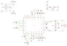
I've made schematic for a BTL version but I have some questions.
Based on this article Understanding output filters for Class-D amplifiers I have designed an output filter. It has a cut off frequency of 19.3KHz.
The article doesn't really say what the differential low pass filter cap (C1 in the article and C5 in my schematic) needs to be in value (some calculations?).
Also what should the 10ohms have in wattage at the power supply? I'm guessing a 0805 standard resistor will do fine since this only needs to drive the non-amplifying internal part of the IC.
Also a little bit stupid question. The large ground plane for this amplifier is GND and not VSSP, right? 😱
Any other changes in my schematic would be handy so I won't need to change too much when I make the PCB due to my low budget right now.
Best regards,
Simon H.A.
I had recently worked with the LME49810 but with a lot of trouble.
Since I have had more luck with Class-D amplifiers I decided to go for a try with the TDA8950 (For a subwoofer).
I learned some more about pcb layout design rules and so for Class-D amplifiers so I should be okay in the layout.
I've made schematic for a BTL version but I have some questions.
Based on this article Understanding output filters for Class-D amplifiers I have designed an output filter. It has a cut off frequency of 19.3KHz.
The article doesn't really say what the differential low pass filter cap (C1 in the article and C5 in my schematic) needs to be in value (some calculations?).
Also what should the 10ohms have in wattage at the power supply? I'm guessing a 0805 standard resistor will do fine since this only needs to drive the non-amplifying internal part of the IC.
Also a little bit stupid question. The large ground plane for this amplifier is GND and not VSSP, right? 😱
Any other changes in my schematic would be handy so I won't need to change too much when I make the PCB due to my low budget right now.
Best regards,
Simon H.A.
Attachments
well
2 things
your cutoff can be a lot lower, since only for sub
2nd thing is, C5 is from what I always seen, the same as capacitor for half bridge, C1, C2 in your case
10R resistors are there not for voltage drop, just some impedance, maybe to create some filtering, but check what Isaa is, how much, is it only supply voltege for IC or some stage
for ground plane, GND is fine, bu could be more complex then that, check IR app notes for IRS2092, there you will find 3, 2 are almost the same, power GND and input GND..3rd is under switches, connected to -Vcc
Last edited:
How low can I cut? I guess it will depend on how large I want the values for the components to be right?
I couldn't find any info on the current drawn from the 10 ohms resistors but they seem not to be used in the power states so I'll guess a 1/4W will do just fine.
C5 will get the same value as C1, C2 etc.
I couldn't find any info on the current drawn from the 10 ohms resistors but they seem not to be used in the power states so I'll guess a 1/4W will do just fine.
C5 will get the same value as C1, C2 etc.
you can cut very low, but since you don't have to go to crazy, 1-2kHz is atleast 10x over what you would need... this also means you could go lower with freq
in your case, C5, I would use 0.7u, since how you have your output filter set up, 2 capacitors are in series, which halfs the total capacitance for them
most of the times I only see C1, C2 and C5 in full bridge config, not one capacitor in series with resistor, but ok also
Oh yes, I forgot to say, I would use 1/4w ones, since it can't have any other usefull job
But would it affect my circuit if I just use 19.3KHz? It's because I have some nice inductors that I would like to use since I've spend a bit money on them.
then use them and don't change, I am just saying what you could do, not what you should do, even more now that you already have parts! leave it at what you wanted it to be in the first place
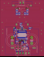
After a lot of work my design is finally done. I have tried to follow the most important design rules as good as possible.
The decoupling capacitors are max. 3 mm from the chip.
I have added as much ground plane as possible on both side and also minimized the use of the bottom side for power and signal tracks.
The inductors are placed 10mm from each other to avoid interference.
I also discovered a error in my schematic which I've fixed.
I have added a lot of via's that I guess will make a good distribution of EMI noise from the top layer to the ground plane on the bottom layer.
Overall I think this look good. What do you think?
Regards,
Simon H.A.
Attachments

I think it looks great, i'm no expert, but looks good to me!
one thing going with higher freq. is that you don't have to use such big inductors, since they cost a lot more then everything else there. just something to think about
one thing going with higher freq. is that you don't have to use such big inductors, since they cost a lot more then everything else there. just something to think about
Thanks and yes I can understand that. It was only because I already had them.
I will change them If I will make more of them.
Regards,
Simon H.A.
I will change them If I will make more of them.
Regards,
Simon H.A.
- Status
- Not open for further replies.
- Home
- Amplifiers
- Class D
- TDA8950 - Could use some design guidance