Have you built the circuit yet?
Thanks for the PCBs 🙂
0.33uF is awfully small as an input cap in the last schematic you posted, and there seems to be <6dB gain. The 1.5kpf input cap seems too large. Overall seems a little wonky, but maybe it's just me.
Thanks for the PCBs 🙂
0.33uF is awfully small as an input cap in the last schematic you posted, and there seems to be <6dB gain. The 1.5kpf input cap seems too large. Overall seems a little wonky, but maybe it's just me.
the pcb bottom layer image posted here looks very very ncie... where did you find it , post the pdf if possible, i m making the one you pdfed earlier,Hi
Here is the non-mirrored bottom ready for toner transfer.
View attachment 149718
Also I found a nice article and schematic for a non inverting configuration with a T-shaped OOS.
![URL]](/community/proxy.php?image=http%3A%2F%2F%5BURL%3Dhttp%3A%2F%2Fimg442.imageshack.us%2Fi%2Ftda7294invertinginput.png%2F%5D%5BIMGDEAD%5Dhttp%3A%2F%2Fimg442.imageshack.us%2Fimg442%2F1637%2Ftda7294invertinginput.png%5B%2FIMGDEAD%5D%5B%2FURL%5D&hash=4125ed3dff47b0703923d77246ccae7b)
I will see if I can find an electronic copy of the schematic.
Wizard
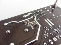
The TDA7294s that I have with me, have all their leads intact (even if they're NC internal to the package). On the PCB layout shown, these NC leads will have to be cut before mounting the package - it's a bit tricky, because they are single-in-line at the package seal, and there's not much room for making clean cuts.
It's probably best to include these pads on the PCB layout and route around them. It reduces the possibility of errors caused by cutting the wrong leads during assembly, etc.
It's probably best to include these pads on the PCB layout and route around them. It reduces the possibility of errors caused by cutting the wrong leads during assembly, etc.
wish you to clarify something
Good work wizard! excellent job! I wish you to clarify on two electrolyte capasitors (1000uF), what I meant was that do I need it if I happened to have two 4700uFs in my PSU? or that just another smooth filter capasitors which are a must? There is nothing to ask more from you, but if you happened to have schematic which has TDA7294 as a driver stage while power transistors as the output stage somewhere betweeb 100 to 200 watt? Thanks Wizard or should I call you "Merlin"!
Best regard
Albert B.
Malaysia
P.S Send my best wish to JK Rowling, if you happen to see her!
Finally figured out how to do attachments
View attachment 149336
View attachment 149337
View attachment 149338

Good work wizard! excellent job! I wish you to clarify on two electrolyte capasitors (1000uF), what I meant was that do I need it if I happened to have two 4700uFs in my PSU? or that just another smooth filter capasitors which are a must? There is nothing to ask more from you, but if you happened to have schematic which has TDA7294 as a driver stage while power transistors as the output stage somewhere betweeb 100 to 200 watt? Thanks Wizard or should I call you "Merlin"!
Best regard
Albert B.
Malaysia
P.S Send my best wish to JK Rowling, if you happen to see her!
Maharaja had foretold
Dear LinuxGuru, the Maharaja told me that you shouldn't have to cut it but just slighty bend it a bit. I gave it a thought of what you said, but Maharaja was right just bend it, in case if you want to reuse that chip again!
The TDA7294s that I have with me, have all their leads intact (even if they're NC internal to the package). On the PCB layout shown, these NC leads will have to be cut before mounting the package - it's a bit tricky, because they are single-in-line at the package seal, and there's not much room for making clean cuts.
It's probably best to include these pads on the PCB layout and route around them. It reduces the possibility of errors caused by cutting the wrong leads during assembly, etc.
Dear LinuxGuru, the Maharaja told me that you shouldn't have to cut it but just slighty bend it a bit. I gave it a thought of what you said, but Maharaja was right just bend it, in case if you want to reuse that chip again!
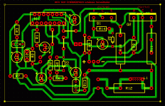
Hello, i made my own version of the pcb of tda7294 and its here. The amp is working, but there are some problems. When i checked the output with oscilloscope it showed that there was distortion in the negative side of the signal. So can anyone help me telling whats causing it, i think there is something wrong in my layout design?? parts values are same as on the datasheet.
[image][/image]
[image]
[image]
Red side is top layer
[image][/image]
[image]
An externally hosted image should be here but it was not working when we last tested it.
[/image][image]
An externally hosted image should be here but it was not working when we last tested it.
[/image]Red side is top layer
Last edited:
Dear Paavi,
Why is your groundplane on the RED layer not connected to the PSU ground?
With kind regards,
Bas
Why is your groundplane on the RED layer not connected to the PSU ground?
With kind regards,
Bas

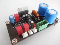
my version of TDA7294 with power transistors 2SC5200 and 2SA1943
This is my version of TDA7294 with power transistors 2SC5200 and 2SA1943. The schematic and the PCB layout is a single zip file and you must have ExpressPCB software to view the files. The amp works fine not unless you feed it with a good preamp. Any suggestions do write to me.
Best regard
Albert B.
Attachments
refer to my post #29
Please refer to my post #29, there you can see PCB layout with all those clean cuts and also some extra power transistors too!
The TDA7294s that I have with me, have all their leads intact (even if they're NC internal to the package). On the PCB layout shown, these NC leads will have to be cut before mounting the package - it's a bit tricky, because they are single-in-line at the package seal, and there's not much room for making clean cuts.
It's probably best to include these pads on the PCB layout and route around them. It reduces the possibility of errors caused by cutting the wrong leads during assembly, etc.
Please refer to my post #29, there you can see PCB layout with all those clean cuts and also some extra power transistors too!
About L1 on the schematic
Thanks for your attention
I have some doubts about your amplifier:
About the L1, how many turns and what is the diameter and which wire to use?
With these power transistors what power i will have and whats the minimum impedance?
Thanks in advance.
Thanks for your attention
I have some doubts about your amplifier:
About the L1, how many turns and what is the diameter and which wire to use?
With these power transistors what power i will have and whats the minimum impedance?
Thanks in advance.
would it not be tempting to separate the power supplies to the input/voltage amplifying stages (pins 7 &8) from the output power stages (pins 13 & 15)? as it has been designed in, and all the pcb's and built amplifiers I have seen don't have this, it may be worth trying. Someone may like it!
Hi sir wizardmaxx,
I am new here and i read your post about your TDA7294 amplifier. and i am interested of it and i want to try to build this circuit, can you give me complete parts list of your TDA7294 amplifier, tnx in advance sir...
I am new here and i read your post about your TDA7294 amplifier. and i am interested of it and i want to try to build this circuit, can you give me complete parts list of your TDA7294 amplifier, tnx in advance sir...
Can I power TDA7294 with single supply +47 VAC transformer? Does anyone have circuit for that?
I would make middle point with resistors. Would it work or do I need to get better middle point?
I would make middle point with resistors. Would it work or do I need to get better middle point?
I am sorry for bumping in but i made a PCB for TDA7293/TDA7294 and i'd like to share it with anyone interested. I have quite a lot of PCB's and selling them for 5 euros a piece including shipping cost to EU. That would be about 3 Euros for a PCB. The power supply caps fitted in the picture are not the ones i intended to use. They are only for testing. The footprint for the caps is 10mm lead spacing and 22mm diameter.
There is a HOT-COLD-GND input connector, an AC-detect/muting connector, a clipping connector for TDA7293 and of course speaker and power supply connectors.
I can also throw in the SMD components for free and can also provide TDA7294 IC's bought from a reputable distributor.
There is a HOT-COLD-GND input connector, an AC-detect/muting connector, a clipping connector for TDA7293 and of course speaker and power supply connectors.
I can also throw in the SMD components for free and can also provide TDA7294 IC's bought from a reputable distributor.
Attachments
Last edited:
- Status
- Not open for further replies.
- Home
- Amplifiers
- Chip Amps
- TDA7294 PCB - Needs Checking