Hi,
Has any body used this DAC solo, ie only one chip instead of the four Kusunoki used? I've tried it with CS8412 Zero OS with a resistor doing the honours I/V wise performance so far is, well, not good! I'm trying different values of R for I/V any experiences out there?
Mozfet😀
Has any body used this DAC solo, ie only one chip instead of the four Kusunoki used? I've tried it with CS8412 Zero OS with a resistor doing the honours I/V wise performance so far is, well, not good! I'm trying different values of R for I/V any experiences out there?
Mozfet😀
hmmm, not yet.
Got a few in my drawer.
You got to use the TDA1307 to convert it to bit stream !
I once heard from an audiophile that he used the bitstream converter with an 7th order filter as DAC.
grtz
Simon
Got a few in my drawer.
You got to use the TDA1307 to convert it to bit stream !
I once heard from an audiophile that he used the bitstream converter with an 7th order filter as DAC.
grtz
Simon
Mozfet,
Tried with one, the objective was to get some sound out of it, not to make the best dac possible.
So i built in into an old philips CD player, hooked it up to the 7210 decoder. Powersupply from the CD player, multipot resistors for i/v conversion (only one chip, 1/4 of the current, resistor needs to be 4 times the value used in the schematics with 4 1543's).
Well it works, but when we tried it at friends installation, we heard some distortion. Could be that his installation does not like the high frequencies. I have to listen more to it to get a better picture (compare it to my marantz '63 1-bit).
What i did learn was that it is interesting enough to proceed with some 1541 S1's i have waiting.
Happy tweaking,
Guido
Simon,
I don't get your post at all ?? A 1543 is the dac and you only need one.. Use an old cd player to get the I2S signals or a crystal receiver. That's it.
Guido
I don't get your post at all ?? A 1543 is the dac and you only need one.. Use an old cd player to get the I2S signals or a crystal receiver. That's it.
Guido
Think that Simon's got the 1547 mixed up with the 1543. The '47 is a BitStream dac and the '43 is a good 'ol cheap 16 bit 8 pin dac. For us in the states Magnavox had a model 462 which was a decoder to dac upsample-filterless player and that was in 1986? It might be fun to poot around on.
agreed!
Well I gotta agree with Jocko Homo on this, it does sound pretty bad, I still like the TDA1541A S1 though! I will try 4 in parallel later.
Mozfet😀
Well I gotta agree with Jocko Homo on this, it does sound pretty bad, I still like the TDA1541A S1 though! I will try 4 in parallel later.
Mozfet😀
Original I ever see 680 Ohms for pin 6 and 8 and pin7 connect by R 330 Ohms .but my friends think the sound is bad he tune R pin 6 and 8 = 512 Ohms and Pin 7 =462 . I think u to try is values.
I ask continous . What voltage to use about TDA1543 I read on TNT he use 8.8 Volt . it max for it and he talk the sound is best.
Who use this value .
I ask continous . What voltage to use about TDA1543 I read on TNT he use 8.8 Volt . it max for it and he talk the sound is best.
Who use this value .
I've used 3 parallel TDA1543's with passive I/V and it sounds very sweet, "open", but thin.
Another experiment with just a singe TDA1543 running at 5V, no bias current (resistor) and this active I/V stage sounds like the passive I/V one, but with more detail and bass, slam and control.
Remember with passive I/V, you give up DAC output voltage compliance bigtime.
Regards, Rudolf.
Another experiment with just a singe TDA1543 running at 5V, no bias current (resistor) and this active I/V stage sounds like the passive I/V one, but with more detail and bass, slam and control.
Remember with passive I/V, you give up DAC output voltage compliance bigtime.
Regards, Rudolf.
Attachments
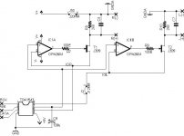
I forgot:
You need to insert resistor (1k or so) from each dac output to ground to get it working and bias the fet as well. No constant current source needed here, the feedback loop keeps dac outputs at voltage compliance.
Opamp type still shines through, I like LM6172 here much more than OPA2604, OPA2134, AD826.
One can also make the opamp a DC servo, I would use CCS then in stead of resistors to draw some bias current.
Use coupling cap for outputs.
Rudolf.
Rudolf,
In your schematic does AGRND connect to GRND through caps? What is the function of jumpers.
With TDA1545 as the DAC you use J309s to provide 1mA bias current to IC and Output J309s - is this all that's needed here?
I am about to implement this for a TDA1545 in a Marantz CD4000 - looking forward to hearing better sounds.
Keep up the good work Rudolf
John
GNDA acts as the +14.2V common for both channels. Didn't figure out a way in Eagle yet to use my own labels...
In stead of the +14.2V you can use GND as common, try it and tell us what you prefer.
Jumper is just there because of my layout in Eagle.
In fact I used the same pcb for the TDA1545A, I included the reference resistors and capacitor.
I wouldn't use a current source at the dac's outputs, but just resistors from each output to the negative rail of -14.2V.
Do install a 8.4672MHz low jitter clock (Elso Kwak's clock for example) in your Marantz. Connect it not only to the transport, but use it as BCK input to the DAC; BCK is running at the same frequency because of 4*(oversampling)* 2(channels)*24(frame width)*44.1kHz=8.4672MHz. This is much better than connecting it to just the transport.
If not installing a seperate clock, do feed the 3 power pins on the SAA737X decoder chip with an individual supply; improvements are better than installing a low jitter clock to the transport only!
I've already had trouble trying to feed a seperate supply to the SAA7378 - the transport behaves erratically - spins v fast but does not sense disk, laser servo clicks, etc. - I believe this has to do with the documented delay needed between the 5V and 12V supply to the transport?
How have u overcome these problems?
I have the KWAK clock schematic and will implement it when I get all the parts.
What about asynchronous clocking of the DAC - have u tried it - is there a schematic available?
Thanks for your help
How have u overcome these problems?
I have the KWAK clock schematic and will implement it when I get all the parts.
What about asynchronous clocking of the DAC - have u tried it - is there a schematic available?
Thanks for your help
Rudolf,
I've built your circuit into one channel of my CDP using the TDA1545A schematic and tried every which way to get it to work but no sounds.
Can you explain
- Is j309 source the pin that loops back to opamp with drain the pin that goes to output?
- V+ can be GND - what is GNDA?
- how to match jfets?
- about waht is the correct value for resistor on J309 giving 1mA sink current?
- Is opamp operating as DC servo in this config & J309 the amplification device?
Hope these questions do not seem stupid but I'm stuck and was looking forward to the sound of this circuit
Regards
John
The fet's drain connects to the I/V resistor, its source to the dac output and feedback loop.
V+ is used as common (signal minus). You could use ground as common as well, though i would prefer V+
You don't need to match the fets and can take any n-fet that has IDDS of say 10mA and up.
Opamp will drive gate of fet, so the voltage on the fets source stays at Vref. So the opamp acts as an active feedback and the fet is more or less a variable resistor with current gain of 1.
I don't remember the exact Vref anymore (something like 3V), but it's safe to take a resistor of about 1k, this should sink a couple of mA which covers the 1mA output swing of the dac AND it's bias current. You can measure the actual Vref on the original opamp output stage, just measure the -input on the opamp.
The circuit I have shown earlier does work, it's from the eagle pcb design package. I've installed it in two players (one with TDA1545A and one with TDA1543). The jfet output stage is also working in a player equiped with TDA1541A-S1...
I do have one pcb left John, so if you don't succeed that's still an option.
About the SAA737X;
I fed the 3 power pins from seperate LM431 shunt regulator supplies that are never switched of. I also augmented some local bypass elco's on the transport and added a bypass elco for the laser supply. No problems.
I'm sorry you're experiencing that many troubles John. Do check all voltages etc. before connecting the dac chip, since you could easily damage it.
Rudolf,
Thank you for your prompt & comprehensive reply
I am using this with the TDA1545A DAC (didn't explain this before)
Please correct any of the following you find to be wrong
I couldn't understand how the right channel had V+ as ground but not on the left channel. The GNDA are not connections to common ground (not connections at all simply symbols?)?
I don't need CCS on DAC output just 1K resistor from each output to neg rail.
I will implement your SAA737X power supply mods - can you help me with which pins I should supply ( should I also supply grounds?)
Pinouts according to SAA7372 datasheet ( no info on SAA7378)
1 - Analog ground 1
2 - Analog supply 1
12 - Analog ground 2
16 - analog ground 3
19 - analog supply 2
30 - Dgital supply 1 for periphery
32 - digital ground 1
39 - digital ground 2
47 - digital supply 2 for periphery
49 - digital ground 3
56 - digital ground 4
59 - digital supply 3 for core
From above analog supply 3 seems to be missing as does digital supply 4 ?
As far as LM431 shunt reg - what is the difference between using 1K+1K, 2K+2K or 3K+3K, etc for 5V regulation?
Sorry about all the questions
regards
John
GNDA in the circuit;
both (-)output are connected to +14.2 volts or so, just labeled GNDA (could be any label if I know how to do it in the pcb design program).
SAA787X
I did use seperate regulators for these.
2 - Analog supply 1
19 - analog supply 2
59 - digital supply 3
But I advise you not to touch them, since you're already experiencing many difficulties getting the output circuit to work.
Success, Rudolf.
- Status
- Not open for further replies.
- Home
- Source & Line
- Digital Source
- TDA1543 anyone tried this?