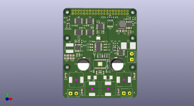
I just finalized my first version of a Raspberry Pi HAT based on the TI TAS5760M. As it's my first amplifier and third PCB I'm hoping for some good feedback on any possible improvements🙂
The intention of the project is to create a wireless multi room speaker system. It should be compact, affordable and with good sound quality, meaning definetly not bad but not neccesary excellent. So quite subjective requirements but hopefully it somewhat describes what I'm aiming for 🙂
I haven't fully finalized the BOM but it should end up at 45€ for the mono and 50€ for the stereo configuration, as the mono configuration can have a depopulated output filter. The design currently has two jumpers to configure the filter part of the layout for stereo or mono setup. I chose the TAS5760 as it accepts I2S as input, configurable to stereo/mono, decent distorsion, powerpad and a fair amount of power.
The board has a fuse and over/under-voltage protection as input power protection. To power all circuits, other than the amplifier power stage, there's a 5V and 3.3V DCDC, LMR33630ADDA and LMR33610ADDA. A PLL1708 generates a master clock for the amplifier. This IC generates various clock signals that are multiple of common audio sampling frequencies. The I2S clocks(Left/Right and Bit) are divided from the master clock using 74HC74 IC:s as frequency dividers. Convertion between 3.3V and 5V logic levels is done with a TXB0104.
I've taken the, what I think is, the easy way by using a 4 layer design as the price doesn't seem to differ that much, currently loking at JLCPCB.
As I'd like a compact design most components are SMD. Most passive components are 0603 as I've previously handsoldered those without to much problems. I'm however a little tempted to use some 0402 capacitors, especially for the bootstrap-capacitors C32-35, as I think the PCB looks a bit crowded there. I've ordered a 0402 practice soldering kit to see if I and my soldering iron is up for the challenge. Is there any drawback or things that require extra attention when using smaller components, with same electrical specifications?
As the PCB currently is larger than the Raspberry Pi footprint I've been thinking of moving some IC:s to the bottom side. This would somewhat complicate my layout with a powerplane divided into different voltages. Are there any other risks with that? Such as noise or EMC?
At some of the smaller filled copper zones on the top layer I've removed the thermal reliefs as the connection becomes quite thin otherwise. Especially the decopuling caps, C22 and C24, on the amplifier. Does this only make it harder to solder or is the wider solid track beneficial?
Any feedback regarding the attached PCB layout is very welcome 🙂
The intention of the project is to create a wireless multi room speaker system. It should be compact, affordable and with good sound quality, meaning definetly not bad but not neccesary excellent. So quite subjective requirements but hopefully it somewhat describes what I'm aiming for 🙂
I haven't fully finalized the BOM but it should end up at 45€ for the mono and 50€ for the stereo configuration, as the mono configuration can have a depopulated output filter. The design currently has two jumpers to configure the filter part of the layout for stereo or mono setup. I chose the TAS5760 as it accepts I2S as input, configurable to stereo/mono, decent distorsion, powerpad and a fair amount of power.
The board has a fuse and over/under-voltage protection as input power protection. To power all circuits, other than the amplifier power stage, there's a 5V and 3.3V DCDC, LMR33630ADDA and LMR33610ADDA. A PLL1708 generates a master clock for the amplifier. This IC generates various clock signals that are multiple of common audio sampling frequencies. The I2S clocks(Left/Right and Bit) are divided from the master clock using 74HC74 IC:s as frequency dividers. Convertion between 3.3V and 5V logic levels is done with a TXB0104.
I've taken the, what I think is, the easy way by using a 4 layer design as the price doesn't seem to differ that much, currently loking at JLCPCB.
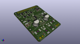
- First layer is signal-layer with a ground pour.
- Second layers is solid ground plane.
- Third layer is powerplane, divided into VDD, 5V and 3.3V.
- Fourth layer is signal layer with ground pour
As I'd like a compact design most components are SMD. Most passive components are 0603 as I've previously handsoldered those without to much problems. I'm however a little tempted to use some 0402 capacitors, especially for the bootstrap-capacitors C32-35, as I think the PCB looks a bit crowded there. I've ordered a 0402 practice soldering kit to see if I and my soldering iron is up for the challenge. Is there any drawback or things that require extra attention when using smaller components, with same electrical specifications?
As the PCB currently is larger than the Raspberry Pi footprint I've been thinking of moving some IC:s to the bottom side. This would somewhat complicate my layout with a powerplane divided into different voltages. Are there any other risks with that? Such as noise or EMC?
At some of the smaller filled copper zones on the top layer I've removed the thermal reliefs as the connection becomes quite thin otherwise. Especially the decopuling caps, C22 and C24, on the amplifier. Does this only make it harder to solder or is the wider solid track beneficial?
Any feedback regarding the attached PCB layout is very welcome 🙂