Tandem regulators are a special class of two-quadrant regulators, in which the series and shunt members do not simply work side-by-side, but cooperate in an active, synergetic manner to sublimate the performances.
I have given details about the principles here (many other topologies are possible, but for the amplifier I will concentrate on a particular one):

These circuits not only work superbly as normal regulators, but thanks to their stiff, accurate output and their source/sink ability, they also do wonders in virtual ground generation
This begs the question: could they work as an output stage?
The answer is yes, and they have exceptional open-loop properties: milliohm output impedance, 0.01% linearity, >>10MHz small signal bandwidth, a fixed, stable and deterministic quiescent current, a <10mV I/O offset, etc.
They look like the dream OP stage, so what's not to love about them?
A few things, unfortunately: there is always a fly or two in any ointment, and this circuit is no exception.
The most obvious quirk is the negative input impedance: around -200 kiloohm at AF frequencies. Not a big deal you might say: connect a 180K in parallel, and the impedance becomes positive, in the megohm range.
You can even use it to change the unity gain buffer into an amplifier: connect the source through a 100K resistor, and the buffer becomes a gain of 2 amplifier; not something I recommend, though.
In addition, the negative impedance is dependent on the Hfe of the input transistor, and since it has a finite Ft, the Hfe and negative resistance will decrease with frequency, requiring additional measures.
The topology also has a more subtle, but annoying feature: a right half-plane zero.
If you look just at Q1, Q5, Q6, ignoring the rest of the circuit, you see an inverting amplifier followed by a common collector buffer, but the whole circuit is in fact a buffer: it does not invert.
This means that for a positive step at the input, the circuit will first try to behave as an inverter, until the ring of the other transistors retakes the control.
Another, more down to earth peculiarity is the difficulty to simulate it reliably: the circuit relies on NFB for DC stability, and positive FB for error correction. The EC (it is a true one, not some NFB in disguise) eliminates all the first-order imperfections.
The rest is a mix of higher order effects, some of which are not well covered in spice simulators and models, which concentrate on the most common effects seen in "ordinary", more conventional circuits.
This means that the sims tend to deviate significantly from the reality: the results are no better or worse, they are simply different, inaccurate.
That is certainly not a valid reason to discard an effective, valuable topology, but it requires more physical verifications.
Manufacturers certainly have better tools at their disposal, like Mextram, and the equivalent of LTspice used internally by ADI is certainly more sophisticated than the public version, but we have to make do with what we have.
Note that this amplifier is just a proof of concept, not a fully-fledged project like the Circlophone, the Old-Fashioned, etc. These projects have been thoroughly studied and designed to be tolerant and almost fool-proof.
This is not the case with this amplifier: you can certainly listen to music through it, but to make it into a serious project would require some homework.
The amplifier can operate in open or closed loop. This is the THD in open-loop mode: 0.04%:

The physical prototype does a little better, 0.03%. The linearity is strongly dependent on the "scaled" matching, and the matching of D1 to Q4 (I have used a diode because using a power transistor to work as a diode looks excessively luxurious).
Various resistors fine-tune the correction: R11, R12 and R14 which forces a positive impedance for the opamp output. As opamp, I have successfully tested NE5534, LT1028 and HA7 2505.
When the GNFB is in service, the THD becomes unmeasurable with my ST1700: it is probably of the order of the ppm, or lower.
Here is the impedance, also open-loop:

The real circuit is slightly worse, at ~10milliohm.
This is the actual prototype:

Here are some pics of the prototype:


And finally, the squarewave response showing the effect of RHP zero on the rising edge

The Tandem stage is very useful building block is you are prepared to develop an amplifier around it.
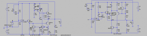
Here is a description of the circuit:
For simplicity, it uses an opamp for the front-end. This limits the output power to ~10W/8ohm.
Q5 and Q2 do the buffering work, and Q4 senses the current through Q2, scales it and applies it to Q5. Since the emitters of Q2 and Q5 follow an analogue I/V relationship, the arrangement eliminates the exponential curvature of the characteristic, linearising the doublet; in theory at least: Q2 and Q5 need to have an intersex, scaled matching. A tall order, with different technologies, junction areas electrons holes mobility, etc.
To fit the curves more closely, corrections are added.
The components selected for the prototype were mainly chosen according to my stock. I have gone overboard with the transistors: the 2N6702 has a Ft of 200Mhz, practically a VHF PA.... The D45H11 is a bit more reasonable at 50MHz, but the BC638 and BD135 from TFK are in the 200~300MHz region. That's asking for trouble, and trouble I had: it is the reason for the hefty ferrite bead.
The first prototype on a breadboard used more sensible BD203/4, had no stability issues and still performed quite well.
The capacitor across the BYV71 might look strange: it is a fast diode, and normally the forward recovery characteristic is excellent, yet it was insufficient in this case, because the circuit pushes some components into their limits
I have given details about the principles here (many other topologies are possible, but for the amplifier I will concentrate on a particular one):
These circuits not only work superbly as normal regulators, but thanks to their stiff, accurate output and their source/sink ability, they also do wonders in virtual ground generation
This begs the question: could they work as an output stage?
The answer is yes, and they have exceptional open-loop properties: milliohm output impedance, 0.01% linearity, >>10MHz small signal bandwidth, a fixed, stable and deterministic quiescent current, a <10mV I/O offset, etc.
They look like the dream OP stage, so what's not to love about them?
A few things, unfortunately: there is always a fly or two in any ointment, and this circuit is no exception.
The most obvious quirk is the negative input impedance: around -200 kiloohm at AF frequencies. Not a big deal you might say: connect a 180K in parallel, and the impedance becomes positive, in the megohm range.
You can even use it to change the unity gain buffer into an amplifier: connect the source through a 100K resistor, and the buffer becomes a gain of 2 amplifier; not something I recommend, though.
In addition, the negative impedance is dependent on the Hfe of the input transistor, and since it has a finite Ft, the Hfe and negative resistance will decrease with frequency, requiring additional measures.
The topology also has a more subtle, but annoying feature: a right half-plane zero.
If you look just at Q1, Q5, Q6, ignoring the rest of the circuit, you see an inverting amplifier followed by a common collector buffer, but the whole circuit is in fact a buffer: it does not invert.
This means that for a positive step at the input, the circuit will first try to behave as an inverter, until the ring of the other transistors retakes the control.
Another, more down to earth peculiarity is the difficulty to simulate it reliably: the circuit relies on NFB for DC stability, and positive FB for error correction. The EC (it is a true one, not some NFB in disguise) eliminates all the first-order imperfections.
The rest is a mix of higher order effects, some of which are not well covered in spice simulators and models, which concentrate on the most common effects seen in "ordinary", more conventional circuits.
This means that the sims tend to deviate significantly from the reality: the results are no better or worse, they are simply different, inaccurate.
That is certainly not a valid reason to discard an effective, valuable topology, but it requires more physical verifications.
Manufacturers certainly have better tools at their disposal, like Mextram, and the equivalent of LTspice used internally by ADI is certainly more sophisticated than the public version, but we have to make do with what we have.
Note that this amplifier is just a proof of concept, not a fully-fledged project like the Circlophone, the Old-Fashioned, etc. These projects have been thoroughly studied and designed to be tolerant and almost fool-proof.
This is not the case with this amplifier: you can certainly listen to music through it, but to make it into a serious project would require some homework.
The amplifier can operate in open or closed loop. This is the THD in open-loop mode: 0.04%:
The physical prototype does a little better, 0.03%. The linearity is strongly dependent on the "scaled" matching, and the matching of D1 to Q4 (I have used a diode because using a power transistor to work as a diode looks excessively luxurious).
Various resistors fine-tune the correction: R11, R12 and R14 which forces a positive impedance for the opamp output. As opamp, I have successfully tested NE5534, LT1028 and HA7 2505.
When the GNFB is in service, the THD becomes unmeasurable with my ST1700: it is probably of the order of the ppm, or lower.
Here is the impedance, also open-loop:
The real circuit is slightly worse, at ~10milliohm.
This is the actual prototype:
Here are some pics of the prototype:
And finally, the squarewave response showing the effect of RHP zero on the rising edge
The Tandem stage is very useful building block is you are prepared to develop an amplifier around it.
Here is a description of the circuit:
For simplicity, it uses an opamp for the front-end. This limits the output power to ~10W/8ohm.
Q5 and Q2 do the buffering work, and Q4 senses the current through Q2, scales it and applies it to Q5. Since the emitters of Q2 and Q5 follow an analogue I/V relationship, the arrangement eliminates the exponential curvature of the characteristic, linearising the doublet; in theory at least: Q2 and Q5 need to have an intersex, scaled matching. A tall order, with different technologies, junction areas electrons holes mobility, etc.
To fit the curves more closely, corrections are added.
The components selected for the prototype were mainly chosen according to my stock. I have gone overboard with the transistors: the 2N6702 has a Ft of 200Mhz, practically a VHF PA.... The D45H11 is a bit more reasonable at 50MHz, but the BC638 and BD135 from TFK are in the 200~300MHz region. That's asking for trouble, and trouble I had: it is the reason for the hefty ferrite bead.
The first prototype on a breadboard used more sensible BD203/4, had no stability issues and still performed quite well.
The capacitor across the BYV71 might look strange: it is a fast diode, and normally the forward recovery characteristic is excellent, yet it was insufficient in this case, because the circuit pushes some components into their limits
Attachments

This looks like fun, have you tried a Tian probe to see what the Return Ratio looks like?
Best wishes
David
Best wishes
David
The Tian probe on the tandem circuit itself makes no sense, because there is no feedback for the signal, just an error-correction return path which adds a tiny positive gain.
Probing the complete amplifier is legitimate, but it will mostly show the characteristic of the opamp used
Probing the complete amplifier is legitimate, but it will mostly show the characteristic of the opamp used
Elvee, so for a bigger amp (with rails e.g. 40V), we would need an input + VAS stages feeding Q5, right?
Instead of traditional input/vas, would it be an option to use floating op-amp, like in your current-dump amp, or is it pushing it too hard?
Instead of traditional input/vas, would it be an option to use floating op-amp, like in your current-dump amp, or is it pushing it too hard?
Yes, you would need a way to supply a signal to Q5, and it has to be low impedance: for the already mentioned reason of the negative impedance, and because this impedance itself is heavily non-linear: you will see it if you plot the base current of Q5 in the sim.
An opamp is ideal for that task, which is why I opted for that solution in my proof of concept.
A floating opamp like my implementation or the one proposed by Mark Tillotson could work, but you would have to take into account the "reaction force" exerted by Q5, and transmitted to the floating supply rails.
Note that it should probably be possible to compensate the non-linear bias current by injecting its opposite: there are places in the structure where the source for such a current could be found, extracted, and transmitted to the base.
Such a bias compensation would greatly ease the drive, and I'll try to come up with a workable solution.
Note that this topology is completely novel, meaning everything remains to be discovered
Also, what about thermal stability? There is no need for idle current control of some kind? Or Q4 limiting current does this job?
I see the idle current is rather high (over 160mA), does it need to be like this?
I see the idle current is rather high (over 160mA), does it need to be like this?
There is no need for thermal compensation: in the actual build, the current is ~60mA.
The current is governed by the CCS around Q6; assuming Q1 requires no base current, all the current will be derived by Q5 (save the current dumped in R10). The current of Q5 is supplied by Q4, which in turn mirrors the current through Q2, divided by the resistors ratio, 10.
Thus, the simplified equation for the quiescent current is ~(Vbe/R1-Vbe/R10)*R3/R2, assuming an infinite Hfe for Q1, and a ratio of 1:10 scaled areas for the junctions of D1 and Q4, and identical non-ideality factors, which is a big ask for two such different devices, but in reality it doesn't matter: it will simply offset the current by some value, but will not affect the stability
The Tian probe on the tandem circuit itself makes no sense, because there is no feedback...
I used the term "Return Ratio" because Bode defined very this carefully, to make sure it made sense independent of any assumptions about feedback (or loops).
Return Ratio is just what comes back if a disturbance is injected into a node.
Obviously useful to analyse a feedback loop but still makes sense in other circuits.
As you wrote in your first post, there is "positive FB for error correction" and it would be educational to see how it works out.
Yes. that was one of the paths I was interested in.just an error-correction return path which adds a tiny positive...
Q6 seems to be in the circuit reversed in your "actual prototype" circuit compared to the first circuits in your post?
Best wishes
David
Ok, I have grounded the input of the tandem, and inserted V4 in the main return path, comprising the DC stabilization and EC paths.I used the term "Return Ratio" because Bode defined very this carefully, to make sure it made sense independent of any assumptions about feedback (or loops).
Return Ratio is just what comes back if a disturbance is injected into a node.
Obviously useful to analyse a feedback loop but still makes sense in other circuits.
As you wrote in your first post, there is "positive FB for error correction" and it would be educational to see how it works out.
I didn't use the full Tian probe, because I feel a bit uneasy with it and I don't want to punch above my weight, but where it is inserted, the impedance at point b is much lower than at point a, thus it should be more than half accurate.
The phase margin seems to be 65°, but the amplitude margin is not visible with 100MHz BW, since I think it should be 180° with this phase-wrapping situation. 0° does not make sense, as it is present from DC to ~100Hz
You are right: the actual circuit is purely graphical, and has been redrawn according to the prototype -with an error or two, unfortunately-Yes. that was one of the paths I was interested in.
Q6 seems to be in the circuit reversed in your "actual prototype" circuit compared to the first circuits in your post?
Best wishes
David
Edit: with 10GHz, I do not manage to reach 180°. Going even higher makes no physical sense for this type of circuit
Last edited:
Minek, I am in the process of analysing your circuit. There is one obvious issue: the high-impedance VAS feeding the negative impedance input, that's a no-no, but fixing that part doesn't solve the problem completely.
I suspect that the RHP zero messes up your carefully crafted compensation scheme
I suspect that the RHP zero messes up your carefully crafted compensation scheme
You know, years ago (back when the DEC in-house audio club used to converse over VT100s) they were touting the benefits of shunt regulation designs regarding how it sounds, I thought the opposite. Why not simply take a big, honkin' power op-amp - like an Apex pa-05 - and just set a DC voltage at the output?This begs the question: could they work as an output stage?
With the ordinary op-amp feedback, that aint going nowhere against +/- load currents...why would it?
It's got your series element for the + current, shunt element for your - current; all in a pre-made package. Of course, there's many other power op-amps than the pa-05...more suitable for line level buffering and preamplification. Just as an "engineering thought" - I never pursued it.
Yes, people have used big amps as 4-quadrant supplies, in test-benches, automatic test systems, etc. Think Crown: their prime business was drivers for vibration shakers
However, these amps have a finite output impedance (very low but not zero) and load stability requirements.
The tandem also has requirements, but if the EC is well balanced, it can have a true zero output impedance (even slightly negative, to compensate for connection resistance) without the usual loop stability requirements.
There is no magic bullet, and no solve-all solution, but having one more option available is always useful
Thanx Elvee. Always something interesting. I'm not sure I understand all the implications of this idea. The not so inverting upper output really had me confused. I have to redraw your schematics so that the bias drops are drawn vertically so my brain to handle them. So far, I have a couple things to say.
1. This regenerative bias maybe the holy grail for diamond amp fans, since it inverts the current waveform in the driver. I plan to try a symmetric buffer to test the idea. You should patent the idea.
2. But for now, I have done a couple simulations. First, you can avoid the inverting signal path by doubling the current mirror and feed the folded cascode driver directly from one of them.
3. I would have called this a power "White buffer". I remember an amplifier in a Canadian magazine about 1969, that claimed such a thing was the ultimate amplifier. It is related to some class-A circuits in DIYA that drive one side based on the emitter resistor drop. For class-AB operation, the slave side of the output derives its input from the idle current of the first, so class-B is not possible. I think maybe this topology is immune to thermal bias issues? So I created a ~crude power White buffer in this simulation for comparison.
Attachments
Too late: it is now published, like all the other finds from my attic1. This regenerative bias maybe the holy grail for diamond amp fans, since it inverts the current waveform in the driver. I plan to try a symmetric buffer to test the idea. You should patent the idea.
Very interesting, it could well solve the RHPZ issue. To be tested.2. But for now, I have done a couple simulations. First, you can avoid the inverting signal path by doubling the current mirror and feed the folded cascode driver directly from one of them.
The controlled lower stage does indeed have many similarities with the White or Taylor topology.3. I would have called this a power "White buffer". I remember an amplifier in a Canadian magazine about 1969, that claimed such a thing was the ultimate amplifier. It is related to some class-A circuits in DIYA that drive one side based on the emitter resistor drop. For class-AB operation, the slave side of the output derives its input from the idle current of the first, so class-B is not possible. I think maybe this topology is immune to thermal bias issues? So I created a ~crude power White buffer in this simulation for comparison.
In UniGabuf, I have pushed the concept to its limits:
https://www.diyaudio.com/community/...er-cut-out-to-be-a-leader.185501/post-2511348
The Tandem does have some unpleasant sides; you could have addressed one of them.
Another one is the close link between the quiescent current and the drive available to the upper transistor; to keep the values reasonable, the Hfe of the upper transistor should be extremely high. A darlington could be a solution, but achieving stability could be difficult.
The negative and highly non-linear input impedance is also a problem, especially if you want to drive the circuit from a conventional VAS.
The solution would be a bias current compensation.
Here is an attempt:
It is rather clumsy and inaccurate though: the compensation depends entirely on the Hfe of Q5 and has to be adjusted with R15.
Ideally, one would like to use the base current of a transistor similar to Q5, subjected to the same collector current, but it looks arduous without undue complications or curtailing the positive swing.
If you have a good idea, it would be welcome
Attachments
Reminds me of OP-07, which current mirrors the base current of a cascode transistor.Too late: it is now published, like all the other finds from my attic
Very interesting, it could well solve the RHPZ issue. To be tested.
The controlled lower stage does indeed have many similarities with the White or Taylor topology.
In UniGabuf, I have pushed the concept to its limits:
https://www.diyaudio.com/community/...er-cut-out-to-be-a-leader.185501/post-2511348
The Tandem does have some unpleasant sides; you could have addressed one of them.
Another one is the close link between the quiescent current and the drive available to the upper transistor; to keep the values reasonable, the Hfe of the upper transistor should be extremely high. A darlington could be a solution, but achieving stability could be difficult.
The negative and highly non-linear input impedance is also a problem, especially if you want to drive the circuit from a conventional VAS.
The solution would be a bias current compensation.
Here is an attempt:
View attachment 1073808
It is rather clumsy and inaccurate though: the compensation depends entirely on the Hfe of Q5 and has to be adjusted with R15.
Ideally, one would like to use the base current of a transistor similar to Q5, subjected to the same collector current, but it looks arduous without undue complications or curtailing the positive swing.
If you have a good idea, it would be welcome
https://www.analog.com/media/en/technical-documentation/data-sheets/OP07.pdf
OP-27 is similar but more complicated.
1. OP-27 mirrors current from another LTP and the cascode transistor is below the input LTP. I'm not sure I understand how it works.
2. If you use a double current mirror, then you could put the cascode transistor in the second mirror instead of in the Q5 collector.
3. But I'm wondering what's wrong with simply adding a load based on the minimum gain of Q5?
4. One of the things I've done is use the driver idle current and not the OP, so the OP can be class-B. The driver can be mostly class-A. But that was a Darlington, not a diamond driver.
5. I'm pondering a lot of possibilities, but I have to draw and simulate them to find a way to make it work. I'm retired and not in any rush.
3. But I'm wondering what's wrong with simply adding a load based on the minimum gain of Q5?
With a high impedance source, like a conventional VAS, this introduces a high level of THD.That's what I did with the static 33K load but it doesn't remove the non-linearity, it simply dilutes it in an offset. It does eliminate the negative resistance though.
So am I....... I'm retired and not in any rush.
I have tested the darlington version: I simply replaced the 2N6702 with a TIP122.
It worked, but for stability, I had to use the base RC compensation and the output Zobel. The compensation harms the crossover, unfortunately. That was expected.
This is the waveform with a 10kHz triangle: a hiccup is clearly visible in the rising part of the waveform.
This is measured in open loop mode. With the loop closed, most of it is polished off, but the goal is to have a pristine response before any FB is applied.
Ideally, a less harmful compensation method should be found, or a way to manipulate the positive drive current without altering the quiescent current. Any smart idea Steve?
Edit: the BC638 still has E and C swapped
Re edit: I included a 0.68 ohm in the zobel, but in fact the capacitor can be connected directly to the output, without impacting the stability.
The Tandem circuit was initially intended as a voltage regulator, and tolerates a high, undamped level of output capacitance
Last edited:
- Home
- Amplifiers
- Solid State
- Tandem-based amplifiers