This project is dedicated to people who think the line preamplifier is an important component of a HiFi chain.
Allow me a warm suggestion to those 5 members who have no respect for enthusiasts sharing their knowledge: please avoid reading this post. Time is precious. Do not waste yours.
Please do not share your “know-it-all” fake knowledge (zero distortion gain stage, Carnot engine kit, sunglasses, and other nonsense). Again: time is precious. Do not waste ours.
I posted some documents about this project in the past, in a nonexclusive thread. That wasn't very clear!
Since many of you have been reaching out to me via private messages, I wanted to share Talia's latest updated version with all of you by collecting all the documents in one place. Forgive me if you read something you already knew.
Forgive me also for the length of this post, it deals with the whole project. The mechanical section is to read only if you want to finalize the project with HiFi2000's Slim-Line 1U/350mm cabinet.
This update was made possible with contributions from some of you, for which I am grateful.
This line preamplifier was born as a running-in bench for the "Shared Gain Stage" (SGS) module I designed mainly for my RIAA preamp/Eq Vera, and I needed to verify and validate it. It would have been hard doing this job on the Vera, which uses 4 SGS modules, so I started Talia's project, which needs only 2.
The SGS module has its roots in an old project of mine, “WOTS Tre” (2008), a cascode of BF244B JFETs with a follower, created to please my friend Gianfranco, who appreciated the sound of my hybrid WOTS LeGrand (2004), but rejected working with tubes. The Tre turned out very well, sporting the same sound as its older brother. I had published it on my website when I had one, and it was built by several enthusiasts, who said they were happy with the realization.
Let's get to the core of the project.
ELECTRONIC SECTION
Objectives set for Talia:
Before proceeding further into the project, I would like to point out that, like the Conrad Johnson GAT, and other prestigious projects, the Talia is inverting. This means that to restore the original phase of the signal, provided your power amplifier is non-inverting, like most of them, the conductors of the speaker cables must be swapped. A non-inverting gain stage could be realized in various ways, which inevitably all lead to non-negligible circuit complications and lengthen the signal path.
Functional blocks:
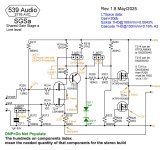
I will not describe the tuning work on the SGS module; from the schematic, you can see a JFET cascode connected with a BJT in CFP configuration (developed by engineer George Clifford Sziklai in the 50s). The BJT increases the JFET cascode's transconductance and its linearity. In this case, we are not looking for a particularly high gain, but we want the amplification stage to be linear across the entire audio band, a fact guaranteed first by the cascode, and then improved by the BJT in CFP.
Which JFETs should I use for the SGS module intended for the Talia? Even if I started with the LSK489A dual JFET to set up the Vera, ending up with excellent results, when I came to set up the Talia, I preferred the LSK489 selection B (LSK489B), which allows an easy configuration for the gain we are interested in. Selection B has a dispersion of the characteristics that is decidedly less wide than selection A. I verified that there is a good chance of being able to match two LSK489Bs acceptably by purchasing only three.
The gain stage is followed by a source follower loaded by a CCS set to 10mA. The depletion MOSFETs seem to be made specifically for the CCS configuration, so I used an IXTP01N100D, which is expensive indeed. According to the opinion of most audiophiles present on various forums, it is one of the best devices for this use. I had some, so I also used them as followers with excellent results. I believe that the cheaper pairs STF3LN80K5/DN2540, and DN2540/DN2540, which do not show any lack of availability, can guarantee the same qualitative results. In other projects, I used the DN2540 with excellent results, but on the net, it is not much appreciated. Sometimes, it happens that a component gets a bad name just because someone has used it badly. A voltage of 60V keeps the JFETs safe, without particular precautions, keeps saturation away, and allows the gain stage to remain linear up to over 10Vrms output signal. Unluckly I lost the LTSpice simulations, and I don't know how to use it fully to replicate the same simulation conditions; I hate its CAD for drawing circuits, but having received the schematic .asc files from a gentle forumer, who is passionate about it, I was able to run several simulations and determine the values of the resistors to use.
A side note: bootstrapping the CFP seems a good idea, but it is not. I tried: the gain increases way too much, and the hiss too. The same behavior is expected if you load the CFP with a CCS.
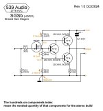
HDP01 module (SGSb - schematic in picture 2, PCB in picture 8).
This is the project by Eng. Maltese presented on the Italian magazine Costruire HiFi #61, which I refer to for the complete discussion of the project. I copied it as is, without changing anything. I have always been attracted to its circuitry. I designed its PCB to be mechanically compatible with that of the SGS.
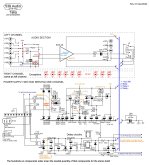
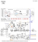
Low pass filter (schematic in picture 3 - motherboard PCB in picture 10). It prevents high-frequency disturbances from reaching the amplification circuits. It is a simple RC circuit housed in the same PCB that connects the hot side of the volume potentiometer to the center pole of the selector and the potentiometer slider to the input of the motherboard.
Virtual Battery power supply (schematic in picture 3, PCB in picture 9). It is the main power supply of the Talia, its circuitry has been known for a long time. I believe it comes from Technics; in my versions, there is always a CCS to drive the Zener diode, preceded by an RC filter. The voltage thus obtained is filtered and sent to a further RC filter, before driving the gate of the output MOSFET. Not being a supporter of feedback, and not requiring a lab instrument precision, my preference for solutions intended for HiFi has always gone to the Virtual Battery circuitry, which has never disappointed me.
60V configuration for the SGS module: set Jp231 open (2&3) and Jp232 closed (2&3). We obtain a 60V output to power the SGS module. Some may wonder why Dz233 is present. Here's the explanation: given the long time constant imposed on the charge of C235, C236 (resistors, capacitors, and the charging current of 1mA), waiting for the voltage to stabilize would become exhausting. Dz233 brings the gate drive voltage almost instantly to the Vin-Vz value, about 40V. Then the voltage continues to rise due to the time constant and the value of the main Zener diode; Dz233 ceases to exist because the voltage at its ends goes below the Zener threshold, and the rise time of the last 20V is entrusted to the time constant mentioned above. This fact is not very decisive in this configuration, which only supplies 60V, but it has its weight when the voltage to be supplied is 300V.
24V configuration for the HDP01 module: to obtain 24V, a voltage suitable for driving the HDP01 module, Jp231 (1&2) must be closed, which puts Dz232 into the circuit at 27V, and consequently Jp232 must be open (1&2), since the “accelerator” function is no longer necessary, indeed, it would overdrive Dz232.
The stabilizer is preceded by a depletion MOSFET connected to the rectifier bridge, configured as CCS, and used as a damper; it limits the turning-on peak and the capacitor charge peaks, and greatly attenuates the disturbances on the power line due to diodes' switching (thanks to Eng. Chiappetta - project Valvolinea). Pay attention to the "Vgs off" of this mosfet (T233), since it determines the value of the resistor connected to its source (R236). The value on the schematic (15Ω) may vary depending on the Vgs off, the goal is to obtain around 72V with load on the + pole of the first capacitor (C231), so vary R236's value according to this.
Delay circuit (schematic in picture 3, PCB in picture 9). It ensures that the output is shorted for approximately 120 seconds from the moment it is turned on. It consists of a timer made with an NE555 and a relay for small currents, whose coil is driven by the NE555 after the time set by the constant R171/C174.
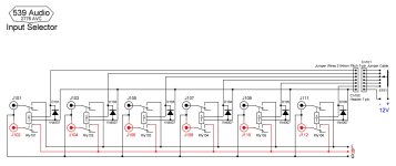
Relay input selector (schematic in picture 4, 2 PCBs in pictures 10 and 11).
It is optional and uses 6 miniature relays with contacts in an inert atmosphere. Their coils are driven by the rotary switch placed on the frame, 1 way, cheap, but reliable. The switch sends to the single relay to be activated the voltage of a power supply similar to that of the delay circuit.
The power supplies of the delay circuit and the input selector have “tube” origin; they use the heater secondary (6.3Vac) by duplicating its voltage to serve the relays. From the schematic, the two power supplies are not evident, it seems to be only one. Being a dual-mono project, the selector power supply is mounted on the PCB of the left channel, and the whole delay block is on the PCB of the right channel. The silkscreens help to understand which components to mount where.
Input and output wiring.
Three solutions are possible for connecting the inputs:
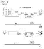
• wired connections, as per the schematic in picture 5, which involves the installation of 12 shielded cables whose braid must be connected only to the ground of the RCA pins, while the opposite end, connected to the selector, does not have the connection of the braid, so a heat-shrink tube must be placed both to isolate the crown of the braid and to mechanically reinforce the central conductor; in this case the selector must be two-way, and of excellent quality; the schematic guarantees a correct path of the signals and the grounds;
• connections made with miniature relays, schematic in picture 4; for the wiring, again consider the schematic in picture 5, starting from the central contact of the selector, which can be cheap, but must be reliable;
• use 12 pieces of unshielded copper wire, of excellent quality, to connect all the inputs to the selector, which in this case must be of excellent quality again.
I chose the first solution, even if the 8 minutes of work for each wire make this activity very boring, which I had to spread out over 3 days. I also see the second solution as a good one, but I have never tried the alternative of unshielded wires; it is used by many DIYers, but I cannot say if it is a good solution.
The last connection to make regarding the input signal is between the volume PCB and the motherboard, also made with a shielded cable, following the wiring schematic.
For the outputs, use the same shielded cable already used for the input signal.
Other wiring.
• connection between IEC socket/fuse holder to transformers: this is made out of a short piece of 3x0.5mm2 mains cable inserted into an antenna cable braiding, connected with the earth conductor only at the end connected with the contact block; everything must be sheathed in a heat-shrink tube; all the conductors are connected to one side of the contact block, the transformer primaries are connected to the opposite side of the contact block;
• connection between the right channel delay circuit and the delay relay on the left channel: this is done with a pair of twisted conductors connected to the appropriate PCB points.
• optional connection between the selector power supply and the relay selector, if you choose this solution.
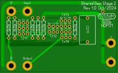
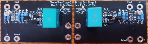
Printed circuit boards. The PCB of the SGS module (pictures 6 and 7, quantity required: 2) is the result of a unique, reversible design to give a symmetrical appearance to the internal assembly of the preamplifier.
IMPORTANT - sometimes the components do not match between the two faces (see T211, R224, and R225); it is not a silkscreen error. Near T213, two jumpers must be made between the two pairs of small SMD pads that are very close to each other; these jumpers swap the G/S of T213, and are made with a drop of tin on the face opposite to the one where the components are mounted. One pair of pads is behind the drain, the other pair is in correspondence with the gate or the source, depending on the face considered. If you forget to activate these jumpers, the module does not work. Thanks to this shrewdness, it was possible to keep the PCB unique, reversible, and symmetrical.
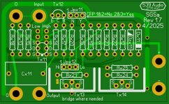
The PCB of the HDP01 module (picture 8, quantity required: 2) is also reversible in symmetry and allows the use of most JFETs and BJTs available on the market.
The PCB of the motherboard (picture 9, quantity required: 2) also derives from a unique, reversible, and symmetrical design: to assemble the two channels, simply mount the components on one face for the left, and on the other face for the right. Since everything is arranged reversibly, except for the NE555 socket, the delay must be mounted on the PCB of the right channel, and the power supply for the selector must be mounted on the PCB of the left channel.
Nothing prevents that, for needs or opinions that I cannot imagine, one uses the same face of the aforementioned PCBs to create the whole assembly, which will then not be symmetrical. In this case, the right faces must be used for both channels, due to the non-reversibility of the NE555 pinout.
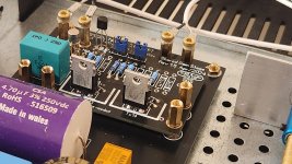
Volume PCB (picture 10, quantity required: 1), solder it directly to the potentiometer; it contains a low-pass filter to eliminate radio frequency disturbances.
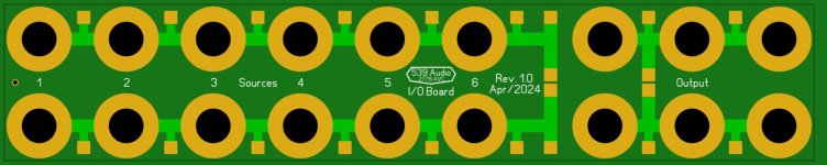
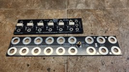
RCA input and output pin PCB for the relay selector solution (picture 11, quantity required: 1): connects the RCA pin grounds and supports the relay PCB.
Relay and RCA pin hot sides PCB (picture 12, quantity required: 1): carries the miniature relays, it is to be soldered to all the RCA pin center connections, and attaches to the PCB below with a screw bringing the mass connection.
RCA input and output pin PCB (picture 13, quantity required: 1): optional, makes it easier to connect to the jack pins in the case of wired assembly.
If you want to build the Talia in a 1U "Slim Line" cabinet by HiFi2000, please read the mechanical notes about it.
Final remarks.
The point “Expected sound” still needs to be developed.
Can I get by with two words?
The best.
Did I get by? No, right?
So I will resume the teachings generously given by the eminent engineer Fulvio Chiappetta on some Costruire HiFi issues, and during his seminars.
Given that distortion cannot be avoided (!) in any circuit, we might as well shape it in a way that is acceptable to our perception. This is a concept that struggles to enter the brains of many pseudo-audiophiles present in significant numbers in the various forums, even here (5 at least). A resilient concept, I would say stubborn, against which there is no logical explanation that holds up. I do not dispense education, I gave up, and I stopped answering those silly questions.
How do you shape distortion? It is not difficult, it is like playing the stock market: buy at the minimum and sell at the maximum. Right? Do not worry, it is not that difficult, it is a matter of finding the polarization of the gain stage that produces the lowest harmonic distortion rate while configuring a monotonically and "appreciably" (I would add) decreasing trend of the amplitude of the harmonics. A system of 2 equations. I will not go into detail here, I do not dare, just search for Engineer Chiappetta's articles, or Google "monotonically decreasing harmonic distortion".
When I calculate a gain stage, sometimes it happens that the total harmonic distortion is very low, that the second harmonic is also very low, but that the third harmonic is slightly higher. I discard the calculation, and go and look for another working point so that the total harmonic distortion could even be higher than that identified before, but the harmonic content presents a third harmonic of amplitude lower than that of the second, the fourth lower than the third, and so on. The term “appreciably” I used in the previous sentence means that I prefer the third harmonic to be significantly below the second, and not a tad below, even if this means a higher THD.
What happens in the Talia?
In the pure cascode configuration, without the contribution of the BJT to form the CFP, LTSpice highlights a THD of 0.16%, which shows a harmonic content mainly of the second harmonic, and monotonically decreasing, in perfect compliance with what was expected. A very “determined” sound, pleasant, thick, never banal, descriptive, at times just flattering.
In the CFP configuration, we have an almost non-existent distortion (0.0043%), whose trend is still favorable. A pure sound, very appreciable, precise and clear, very clean, never abundant, never harsh. But the soundstage "seems" to be slightly less coherent over time compared to that offered by the pure cascode, the instruments move a bit. These are my impressions. We are entering the field of psychoacoustics, and I stop here.
I am going to trivialize, and I venture a summary of the listening experience: we like this kind of distortion! The instruments are placed without hesitation, and they remain there. And I knew this, from the many positive reviews that had come to me from those who had built the WOTS Le Grand and the Tre, which by their nature dispense that very welcome harmonic content. Hey, 5 fellas! I told you where to stop reading. What are you still doing here? Trying to learn something? Don't say, don't waste our time, inform yourself, please. Even Google's AI knows!
The two configurations, pure cascode and CFP, are obtained by moving the JP211 jumper; the pure cascode has a slightly lower gain than the CFP configuration.
I'm sorry for the enthusiasts (mainly Italian), I have not yet conducted an exhaustive listening test with the HDP01 module. When tested by switching it on and listening for a very short time, it works perfectly, and I'm sure that it maintains without difficulty what Eng. Maltese said in his presentation. To me, it is a very interesting solution.
The text was too long, so I had to split it. The following posts will end the description of the project.
Allow me a warm suggestion to those 5 members who have no respect for enthusiasts sharing their knowledge: please avoid reading this post. Time is precious. Do not waste yours.
Please do not share your “know-it-all” fake knowledge (zero distortion gain stage, Carnot engine kit, sunglasses, and other nonsense). Again: time is precious. Do not waste ours.
I posted some documents about this project in the past, in a nonexclusive thread. That wasn't very clear!
Since many of you have been reaching out to me via private messages, I wanted to share Talia's latest updated version with all of you by collecting all the documents in one place. Forgive me if you read something you already knew.
Forgive me also for the length of this post, it deals with the whole project. The mechanical section is to read only if you want to finalize the project with HiFi2000's Slim-Line 1U/350mm cabinet.
This update was made possible with contributions from some of you, for which I am grateful.
This line preamplifier was born as a running-in bench for the "Shared Gain Stage" (SGS) module I designed mainly for my RIAA preamp/Eq Vera, and I needed to verify and validate it. It would have been hard doing this job on the Vera, which uses 4 SGS modules, so I started Talia's project, which needs only 2.
The SGS module has its roots in an old project of mine, “WOTS Tre” (2008), a cascode of BF244B JFETs with a follower, created to please my friend Gianfranco, who appreciated the sound of my hybrid WOTS LeGrand (2004), but rejected working with tubes. The Tre turned out very well, sporting the same sound as its older brother. I had published it on my website when I had one, and it was built by several enthusiasts, who said they were happy with the realization.
Let's get to the core of the project.
ELECTRONIC SECTION
Objectives set for Talia:
- simplicity and effectiveness: a single gain stage;
- use of the SGS module configured for a “line” gain of about 20db;
- dual-mono construction, only the mass is in common between left and right channels, and should not be separated;
- slim aesthetics (19" 1U) because I like it, and it does not weigh down the area of the audio system;
- possibility of deactivating the BJT of the CFP, leaving only the JFET cascode active;
- no loop feedback, only local feedback;
- stabilized power supply without feedback;
- this point was an old obsession of mine: the possibility of replacing the SGS module with the HDP01 module by Eng. Maltese (Italian magazine Costruire HiFi #61), configuring the motherboard for a voltage of 24V;
- expected sound: I will deal with it later.
Before proceeding further into the project, I would like to point out that, like the Conrad Johnson GAT, and other prestigious projects, the Talia is inverting. This means that to restore the original phase of the signal, provided your power amplifier is non-inverting, like most of them, the conductors of the speaker cables must be swapped. A non-inverting gain stage could be realized in various ways, which inevitably all lead to non-negligible circuit complications and lengthen the signal path.
Functional blocks:
- SGSa or HDP01 (SGSb) module for signal amplification;
- low-pass filter at the input, inserted in the volume potentiometer board;
- Virtual Battery type power supply;
- delay circuit that keeps the output short for about 120 seconds from power on;
- input selector (optional) made with miniature relays, and a small power supply.
I will not describe the tuning work on the SGS module; from the schematic, you can see a JFET cascode connected with a BJT in CFP configuration (developed by engineer George Clifford Sziklai in the 50s). The BJT increases the JFET cascode's transconductance and its linearity. In this case, we are not looking for a particularly high gain, but we want the amplification stage to be linear across the entire audio band, a fact guaranteed first by the cascode, and then improved by the BJT in CFP.
Which JFETs should I use for the SGS module intended for the Talia? Even if I started with the LSK489A dual JFET to set up the Vera, ending up with excellent results, when I came to set up the Talia, I preferred the LSK489 selection B (LSK489B), which allows an easy configuration for the gain we are interested in. Selection B has a dispersion of the characteristics that is decidedly less wide than selection A. I verified that there is a good chance of being able to match two LSK489Bs acceptably by purchasing only three.
The gain stage is followed by a source follower loaded by a CCS set to 10mA. The depletion MOSFETs seem to be made specifically for the CCS configuration, so I used an IXTP01N100D, which is expensive indeed. According to the opinion of most audiophiles present on various forums, it is one of the best devices for this use. I had some, so I also used them as followers with excellent results. I believe that the cheaper pairs STF3LN80K5/DN2540, and DN2540/DN2540, which do not show any lack of availability, can guarantee the same qualitative results. In other projects, I used the DN2540 with excellent results, but on the net, it is not much appreciated. Sometimes, it happens that a component gets a bad name just because someone has used it badly. A voltage of 60V keeps the JFETs safe, without particular precautions, keeps saturation away, and allows the gain stage to remain linear up to over 10Vrms output signal. Unluckly I lost the LTSpice simulations, and I don't know how to use it fully to replicate the same simulation conditions; I hate its CAD for drawing circuits, but having received the schematic .asc files from a gentle forumer, who is passionate about it, I was able to run several simulations and determine the values of the resistors to use.
A side note: bootstrapping the CFP seems a good idea, but it is not. I tried: the gain increases way too much, and the hiss too. The same behavior is expected if you load the CFP with a CCS.
HDP01 module (SGSb - schematic in picture 2, PCB in picture 8).
This is the project by Eng. Maltese presented on the Italian magazine Costruire HiFi #61, which I refer to for the complete discussion of the project. I copied it as is, without changing anything. I have always been attracted to its circuitry. I designed its PCB to be mechanically compatible with that of the SGS.
Low pass filter (schematic in picture 3 - motherboard PCB in picture 10). It prevents high-frequency disturbances from reaching the amplification circuits. It is a simple RC circuit housed in the same PCB that connects the hot side of the volume potentiometer to the center pole of the selector and the potentiometer slider to the input of the motherboard.
Virtual Battery power supply (schematic in picture 3, PCB in picture 9). It is the main power supply of the Talia, its circuitry has been known for a long time. I believe it comes from Technics; in my versions, there is always a CCS to drive the Zener diode, preceded by an RC filter. The voltage thus obtained is filtered and sent to a further RC filter, before driving the gate of the output MOSFET. Not being a supporter of feedback, and not requiring a lab instrument precision, my preference for solutions intended for HiFi has always gone to the Virtual Battery circuitry, which has never disappointed me.
60V configuration for the SGS module: set Jp231 open (2&3) and Jp232 closed (2&3). We obtain a 60V output to power the SGS module. Some may wonder why Dz233 is present. Here's the explanation: given the long time constant imposed on the charge of C235, C236 (resistors, capacitors, and the charging current of 1mA), waiting for the voltage to stabilize would become exhausting. Dz233 brings the gate drive voltage almost instantly to the Vin-Vz value, about 40V. Then the voltage continues to rise due to the time constant and the value of the main Zener diode; Dz233 ceases to exist because the voltage at its ends goes below the Zener threshold, and the rise time of the last 20V is entrusted to the time constant mentioned above. This fact is not very decisive in this configuration, which only supplies 60V, but it has its weight when the voltage to be supplied is 300V.
24V configuration for the HDP01 module: to obtain 24V, a voltage suitable for driving the HDP01 module, Jp231 (1&2) must be closed, which puts Dz232 into the circuit at 27V, and consequently Jp232 must be open (1&2), since the “accelerator” function is no longer necessary, indeed, it would overdrive Dz232.
The stabilizer is preceded by a depletion MOSFET connected to the rectifier bridge, configured as CCS, and used as a damper; it limits the turning-on peak and the capacitor charge peaks, and greatly attenuates the disturbances on the power line due to diodes' switching (thanks to Eng. Chiappetta - project Valvolinea). Pay attention to the "Vgs off" of this mosfet (T233), since it determines the value of the resistor connected to its source (R236). The value on the schematic (15Ω) may vary depending on the Vgs off, the goal is to obtain around 72V with load on the + pole of the first capacitor (C231), so vary R236's value according to this.
Delay circuit (schematic in picture 3, PCB in picture 9). It ensures that the output is shorted for approximately 120 seconds from the moment it is turned on. It consists of a timer made with an NE555 and a relay for small currents, whose coil is driven by the NE555 after the time set by the constant R171/C174.
Relay input selector (schematic in picture 4, 2 PCBs in pictures 10 and 11).
It is optional and uses 6 miniature relays with contacts in an inert atmosphere. Their coils are driven by the rotary switch placed on the frame, 1 way, cheap, but reliable. The switch sends to the single relay to be activated the voltage of a power supply similar to that of the delay circuit.
The power supplies of the delay circuit and the input selector have “tube” origin; they use the heater secondary (6.3Vac) by duplicating its voltage to serve the relays. From the schematic, the two power supplies are not evident, it seems to be only one. Being a dual-mono project, the selector power supply is mounted on the PCB of the left channel, and the whole delay block is on the PCB of the right channel. The silkscreens help to understand which components to mount where.
Input and output wiring.
Three solutions are possible for connecting the inputs:
• wired connections, as per the schematic in picture 5, which involves the installation of 12 shielded cables whose braid must be connected only to the ground of the RCA pins, while the opposite end, connected to the selector, does not have the connection of the braid, so a heat-shrink tube must be placed both to isolate the crown of the braid and to mechanically reinforce the central conductor; in this case the selector must be two-way, and of excellent quality; the schematic guarantees a correct path of the signals and the grounds;
• connections made with miniature relays, schematic in picture 4; for the wiring, again consider the schematic in picture 5, starting from the central contact of the selector, which can be cheap, but must be reliable;
• use 12 pieces of unshielded copper wire, of excellent quality, to connect all the inputs to the selector, which in this case must be of excellent quality again.
I chose the first solution, even if the 8 minutes of work for each wire make this activity very boring, which I had to spread out over 3 days. I also see the second solution as a good one, but I have never tried the alternative of unshielded wires; it is used by many DIYers, but I cannot say if it is a good solution.
The last connection to make regarding the input signal is between the volume PCB and the motherboard, also made with a shielded cable, following the wiring schematic.
For the outputs, use the same shielded cable already used for the input signal.
Other wiring.
• connection between IEC socket/fuse holder to transformers: this is made out of a short piece of 3x0.5mm2 mains cable inserted into an antenna cable braiding, connected with the earth conductor only at the end connected with the contact block; everything must be sheathed in a heat-shrink tube; all the conductors are connected to one side of the contact block, the transformer primaries are connected to the opposite side of the contact block;
• connection between the right channel delay circuit and the delay relay on the left channel: this is done with a pair of twisted conductors connected to the appropriate PCB points.
• optional connection between the selector power supply and the relay selector, if you choose this solution.
Printed circuit boards. The PCB of the SGS module (pictures 6 and 7, quantity required: 2) is the result of a unique, reversible design to give a symmetrical appearance to the internal assembly of the preamplifier.
IMPORTANT - sometimes the components do not match between the two faces (see T211, R224, and R225); it is not a silkscreen error. Near T213, two jumpers must be made between the two pairs of small SMD pads that are very close to each other; these jumpers swap the G/S of T213, and are made with a drop of tin on the face opposite to the one where the components are mounted. One pair of pads is behind the drain, the other pair is in correspondence with the gate or the source, depending on the face considered. If you forget to activate these jumpers, the module does not work. Thanks to this shrewdness, it was possible to keep the PCB unique, reversible, and symmetrical.
The PCB of the HDP01 module (picture 8, quantity required: 2) is also reversible in symmetry and allows the use of most JFETs and BJTs available on the market.
The PCB of the motherboard (picture 9, quantity required: 2) also derives from a unique, reversible, and symmetrical design: to assemble the two channels, simply mount the components on one face for the left, and on the other face for the right. Since everything is arranged reversibly, except for the NE555 socket, the delay must be mounted on the PCB of the right channel, and the power supply for the selector must be mounted on the PCB of the left channel.
Nothing prevents that, for needs or opinions that I cannot imagine, one uses the same face of the aforementioned PCBs to create the whole assembly, which will then not be symmetrical. In this case, the right faces must be used for both channels, due to the non-reversibility of the NE555 pinout.
Volume PCB (picture 10, quantity required: 1), solder it directly to the potentiometer; it contains a low-pass filter to eliminate radio frequency disturbances.
RCA input and output pin PCB for the relay selector solution (picture 11, quantity required: 1): connects the RCA pin grounds and supports the relay PCB.
Relay and RCA pin hot sides PCB (picture 12, quantity required: 1): carries the miniature relays, it is to be soldered to all the RCA pin center connections, and attaches to the PCB below with a screw bringing the mass connection.
RCA input and output pin PCB (picture 13, quantity required: 1): optional, makes it easier to connect to the jack pins in the case of wired assembly.
If you want to build the Talia in a 1U "Slim Line" cabinet by HiFi2000, please read the mechanical notes about it.
Final remarks.
The point “Expected sound” still needs to be developed.
Can I get by with two words?
The best.
Did I get by? No, right?
So I will resume the teachings generously given by the eminent engineer Fulvio Chiappetta on some Costruire HiFi issues, and during his seminars.
Given that distortion cannot be avoided (!) in any circuit, we might as well shape it in a way that is acceptable to our perception. This is a concept that struggles to enter the brains of many pseudo-audiophiles present in significant numbers in the various forums, even here (5 at least). A resilient concept, I would say stubborn, against which there is no logical explanation that holds up. I do not dispense education, I gave up, and I stopped answering those silly questions.
How do you shape distortion? It is not difficult, it is like playing the stock market: buy at the minimum and sell at the maximum. Right? Do not worry, it is not that difficult, it is a matter of finding the polarization of the gain stage that produces the lowest harmonic distortion rate while configuring a monotonically and "appreciably" (I would add) decreasing trend of the amplitude of the harmonics. A system of 2 equations. I will not go into detail here, I do not dare, just search for Engineer Chiappetta's articles, or Google "monotonically decreasing harmonic distortion".
When I calculate a gain stage, sometimes it happens that the total harmonic distortion is very low, that the second harmonic is also very low, but that the third harmonic is slightly higher. I discard the calculation, and go and look for another working point so that the total harmonic distortion could even be higher than that identified before, but the harmonic content presents a third harmonic of amplitude lower than that of the second, the fourth lower than the third, and so on. The term “appreciably” I used in the previous sentence means that I prefer the third harmonic to be significantly below the second, and not a tad below, even if this means a higher THD.
What happens in the Talia?
In the pure cascode configuration, without the contribution of the BJT to form the CFP, LTSpice highlights a THD of 0.16%, which shows a harmonic content mainly of the second harmonic, and monotonically decreasing, in perfect compliance with what was expected. A very “determined” sound, pleasant, thick, never banal, descriptive, at times just flattering.
In the CFP configuration, we have an almost non-existent distortion (0.0043%), whose trend is still favorable. A pure sound, very appreciable, precise and clear, very clean, never abundant, never harsh. But the soundstage "seems" to be slightly less coherent over time compared to that offered by the pure cascode, the instruments move a bit. These are my impressions. We are entering the field of psychoacoustics, and I stop here.
I am going to trivialize, and I venture a summary of the listening experience: we like this kind of distortion! The instruments are placed without hesitation, and they remain there. And I knew this, from the many positive reviews that had come to me from those who had built the WOTS Le Grand and the Tre, which by their nature dispense that very welcome harmonic content. Hey, 5 fellas! I told you where to stop reading. What are you still doing here? Trying to learn something? Don't say, don't waste our time, inform yourself, please. Even Google's AI knows!
The two configurations, pure cascode and CFP, are obtained by moving the JP211 jumper; the pure cascode has a slightly lower gain than the CFP configuration.
I'm sorry for the enthusiasts (mainly Italian), I have not yet conducted an exhaustive listening test with the HDP01 module. When tested by switching it on and listening for a very short time, it works perfectly, and I'm sure that it maintains without difficulty what Eng. Maltese said in his presentation. To me, it is a very interesting solution.
The text was too long, so I had to split it. The following posts will end the description of the project.

The esoteric corner.
And now, under the aegis of the usual rule of the "scarrafone" (google "regola dello scarrafone", and translate the results in your language), I am here to declare without shame that the new PCB that houses the depletion MOSFET after the rectifier bridge, gives the Talia a sound of superior quality to its hybrid colleagues. Why? I remember that a few years ago, Mauro of the Audiokit shop asked me if I could hear differences between “position A” and “position B”. It was hard to say which one was better, but there were differences, indeed. What was Mauro swapping? He swapped the SPDIF connection cable (about 1 meter) between the CD player and the DAC. How can a cable where the “0s” and the “1s” pass through make a difference? And here, on the Talia, how can a CCS inserted on the Vpuls, before the Virtual Battery, which stabilizes and filters everything, make such a big difference? In this case, there is no uncertainty better/worse of the different results, there is only the better. Try it and believe it, keeping in mind the title of this paragraph.
I'm keeping the Talia configured with the CFP active, and I am fully satisfied. The new PCBs with the CCS are also ready for the hybrid preamps; we will see.
Conclusions.
Talia's electronic assembly is very simple once you have the PCBs. There are no acrobatics to do when mounting the assembly in the cabinet.
The mechanical part is medium demanding, requiring the use of a column drill for the holes of the front and back panels. Alternatively, you can rely on HiFi2000 to drill the front panel and the rear panel with or without writings/engravings.
By following the instructions in the next section, it is possible to get hold of a significant preamplifier with excellent performance and a very attractive, sober, and essential aesthetic.
The following are available for non-profit purposes:
and ask for my PCB and schematics original files.
Maybe you have to refine the value of R216 and R219 depending on the characteristics of your LSK489Bs, the goal is to obtain something less than 30V on the emitter of T212. Please do not ask me for LSK489B (which is THE core component) alternatives, but try at your own experience and risk, and post your findings.
Thanks to:
IMPORTANT DISCLAIMER STATEMENT:
Aside from the mains voltage, present in some points of the assembly in question, and which is dangerous to health to the point of being fatal, the voltages present after the secondary windings of the transformers and in the circuits of this project are annoying but generally not harmful to health in completely healthy subjects, if there is an exposure that ends with a reflex arc reaction. Conversely, they could be dangerous to health and could cause the death of subjects with confirmed or hidden pathologies. The reader is warned. The author declines any responsibility arising from the consequences of having undertaken the activities described and underlying here.
Pictures:
MECHANICAL SECTION
The following text is dedicated to those who want to use the Slim Line cabinet by HiFi2000 1U/350mm. You can skip this reading if you are considering using a different cabinet.
The Cabinet chosen is the Slim Line 1U by HiFi2000, 350mm deep (1NSLA01350N), with a 10mm thick front panel and 3mm aluminum full vented upper and lower panels and a 1BASE0105MAX mounting base, not 1BASE0105ULTRA, which did not yet exist at the time of my construction; it could be a valid choice, but I cannot guarantee it. The knobs are again by HiFi2000, black, one 24.5mm (selector) and one 39.5mm (potentiometer), on whose bezels I put a drop of red insulating paint.
The effort to be put into the mechanics of this project is not particularly burdensome, but it is still not negligible. You need to have a pillar drill and excellent quality bits. Or entrust the drilling to a service (I use HiFi2000), if you also want the engravings and printings.
The layout inside the cabinet reflects the setting I gave to all my pre-line amplifiers, to keep the wiring as short as possible. This forces the positioning of the potentiometer and the selector in the rear part of the cabinet. This implies the need to extend the potentiometer and selector stems with two pieces of rod (eBay), until they protrude from the front panel and then end them with a pair of knobs. Then comes into play a 1.25” x 1.25” x 1/16” (thickness) aluminum angle (eBay) on which the potentiometer and selector are fixed. I will not go further in the description of the mechanics, the photos give a better idea than many words.
Some suggestions for precise workmanship:
And now, under the aegis of the usual rule of the "scarrafone" (google "regola dello scarrafone", and translate the results in your language), I am here to declare without shame that the new PCB that houses the depletion MOSFET after the rectifier bridge, gives the Talia a sound of superior quality to its hybrid colleagues. Why? I remember that a few years ago, Mauro of the Audiokit shop asked me if I could hear differences between “position A” and “position B”. It was hard to say which one was better, but there were differences, indeed. What was Mauro swapping? He swapped the SPDIF connection cable (about 1 meter) between the CD player and the DAC. How can a cable where the “0s” and the “1s” pass through make a difference? And here, on the Talia, how can a CCS inserted on the Vpuls, before the Virtual Battery, which stabilizes and filters everything, make such a big difference? In this case, there is no uncertainty better/worse of the different results, there is only the better. Try it and believe it, keeping in mind the title of this paragraph.
I'm keeping the Talia configured with the CFP active, and I am fully satisfied. The new PCBs with the CCS are also ready for the hybrid preamps; we will see.
Conclusions.
Talia's electronic assembly is very simple once you have the PCBs. There are no acrobatics to do when mounting the assembly in the cabinet.
The mechanical part is medium demanding, requiring the use of a column drill for the holes of the front and back panels. Alternatively, you can rely on HiFi2000 to drill the front panel and the rear panel with or without writings/engravings.
By following the instructions in the next section, it is possible to get hold of a significant preamplifier with excellent performance and a very attractive, sober, and essential aesthetic.
The following are available for non-profit purposes:
- Gerber files to send to the service that produces the PCBs (I use JLCPCB);
- drilling masks of the angle in Sprint Layout format (PCB CAD by Abacom, of which you can download the demo version for free, which should allow printing), or at least the visualization to check the measurements;
- CAD drawings of the front and rear panel machining to send to the service (I use HiFi2000);
- list of components in spreadsheet format, which shows the Mouser codes, and allows you to load the last 2 columns in a Mouser BOM, or the third and last column in a BOM of any other distributor by keying on the MFR code. The components indicated in the list are certainly compatible with the PCBs.
- Notice that the CAD drawing of the front panel does not report any drilling, but only the engraving of the center of the two holes. This allows you to save some money, but you have to drill yourself, like I did,
and ask for my PCB and schematics original files.
Maybe you have to refine the value of R216 and R219 depending on the characteristics of your LSK489Bs, the goal is to obtain something less than 30V on the emitter of T212. Please do not ask me for LSK489B (which is THE core component) alternatives, but try at your own experience and risk, and post your findings.
Thanks to:
- my dear friend Flavio Annecchiarico, whose knowledge is complementary to mine, and who supported me, unfortunately, from a long way away, even in this creation that he will never be able to listen to, unless he builds it himself;
- HiFi2000 for the high quality of the cabinets and workmanship;
- JLCPCB for the consistency of the excellent quality of the PCBs and the speed of delivery (very expensive indeed), at least here in the USA;
- special thanks to members @wwwtttwww for introducing me to LTSpice, and @PANDINUS for intercepting the numerous typos on the schematic, PCBs, and text.
IMPORTANT DISCLAIMER STATEMENT:
Aside from the mains voltage, present in some points of the assembly in question, and which is dangerous to health to the point of being fatal, the voltages present after the secondary windings of the transformers and in the circuits of this project are annoying but generally not harmful to health in completely healthy subjects, if there is an exposure that ends with a reflex arc reaction. Conversely, they could be dangerous to health and could cause the death of subjects with confirmed or hidden pathologies. The reader is warned. The author declines any responsibility arising from the consequences of having undertaken the activities described and underlying here.
Pictures:
- 01 – SGSs module schematic.
- 02 – HDP01 (SGSb) module schematic.
- 03 – Mainboard schematic including the Low Pass Filter, Power Supply, Delay, and Power Supply functional blocks for the relay selector.
- 04 – Schematic of Sources Board Input Selector 5.1 (Relay input selector).
- 05 – input wiring schematic. If you choose the relay selector, consider the schematic starting from the central contact of the selector.
- 06 – PCB of the SGS module left channel.
- 07 – PCB of the SGS module right channel. This is the same PCB as in picture 6, turned on the opposite side. In order not to take up too much space, the other double-sided PCBs will be shown only on the left channel side.
- 08 – PCB of the HDP01 module, left channel side. Turning the PCB over, the right channel side shows.
- 09 – PCB of the motherboard, left channel side. Turning the PCB over, the right channel side shows.
- 10 – PCB of the volume board, with the low-pass filter. It must be soldered to the potentiometer.
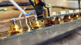
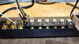
- 11 – PCB for connecting the RCA pins, it is mechanically in contact with the rear panel, and makes it possible to connect to the input PCB in picture 12. An 8mm long M3 threaded female/female brass turret (pics 16/17/18/19) must be soldered on the SMD pad.
- 12 – relay PCB for connecting the hot sides of the RCA pins. It is soldered on the hot sides of the RCA pins; a brass turret male/female (pic 18) must be inserted into the hole corresponding to the brass turret of the underlying board. The photos of the installation clarify the assembly.
- 13 – PCB for connecting the RCA pins, which is mechanically in contact with the rear panel, and facilitates the connection of the jack pins. It is optional and is not suitable for working with the relay selector, for which the PCB in picture 11 must be chosen.
- 14 – Zoom in on the SGS module mounted in service. The PCB in the photo is from V.1.5, the current one is V1.7, which has only one jumper for cascode/CFP switching
- 15 – left and right HDP01 modules.
- 16 – Mounting PCBs of the relay input selector.
- 17 – Detail of the RCA pin mounting PCB, showing the brass turret soldered to the PCB, which, in addition to providing mechanical support to the relay PCB, carries the ground.
- 18 – Shows the installation of the two “RCA pin” and “relay” PCBs. Since my Talia uses the wired selector, I included the photo of another hybrid preamp, which is why you can see a fan. The selector in the photo is of excellent quality, wasted in this case.
- 19 – I tried to highlight the turret that mechanically and electrically connects the two PCBs.
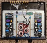
- 20 – Top view of the inside of the preamplifier. 2 of the 3 10VA transformers have two 30Vac secondaries connected in series, and serve the main power supply; the third transformer has two 6Vac secondaries, which power the services. This is not a mandatory solution, it is simply what I found available.
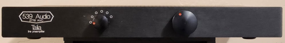
- 21 – Front view. Notice the extreme essentiality of the front panel that does not attack the eye with lights and a high density of elements. The writings are engraved.
- 22 – Rear view. The writings are printed.
MECHANICAL SECTION
The following text is dedicated to those who want to use the Slim Line cabinet by HiFi2000 1U/350mm. You can skip this reading if you are considering using a different cabinet.
The Cabinet chosen is the Slim Line 1U by HiFi2000, 350mm deep (1NSLA01350N), with a 10mm thick front panel and 3mm aluminum full vented upper and lower panels and a 1BASE0105MAX mounting base, not 1BASE0105ULTRA, which did not yet exist at the time of my construction; it could be a valid choice, but I cannot guarantee it. The knobs are again by HiFi2000, black, one 24.5mm (selector) and one 39.5mm (potentiometer), on whose bezels I put a drop of red insulating paint.
The effort to be put into the mechanics of this project is not particularly burdensome, but it is still not negligible. You need to have a pillar drill and excellent quality bits. Or entrust the drilling to a service (I use HiFi2000), if you also want the engravings and printings.
The layout inside the cabinet reflects the setting I gave to all my pre-line amplifiers, to keep the wiring as short as possible. This forces the positioning of the potentiometer and the selector in the rear part of the cabinet. This implies the need to extend the potentiometer and selector stems with two pieces of rod (eBay), until they protrude from the front panel and then end them with a pair of knobs. Then comes into play a 1.25” x 1.25” x 1/16” (thickness) aluminum angle (eBay) on which the potentiometer and selector are fixed. I will not go further in the description of the mechanics, the photos give a better idea than many words.
Some suggestions for precise workmanship:
- it is assumed that all the work required for the front and rear panel has been carried out;
- to fix the PCBs to the base use 12 M3 brass turrets, 5mm high, 6mm threaded stem (eBay) that must be fixed to the base with the same number of M3 flat-head screws, 5mm long; be careful to cut all the leads protruding from the PCBs as short as possible;
- buy (eBay) 2 brass bushings for the passage of the shafts with an internal diameter equal to that of the shafts (the diameter of my shafts is 6.3mm, and the external diameter of my bushings is 9.55mm);
- buy (eBay) the shaft/potentiometer and shaft/selector connections and machine them, if necessary, to accommodate the component stem on one side, and the shaft on the other;
- on the front panel, make two holes equal to the external diameter of the bushings and insert the bushings using a hammer and a piece of wood, use a file if necessary, if the holes are smaller, or with a two-component glue if the holes are larger (smaller or larger means a tolerance of 1 tenth of a mm);
- mount some M3 flat-head screws on the base of the cabinet: a pair in the center, three on a line parallel and close to the front panel, 1 on the left, 1 in the center, 1 on the right, another 3 on a line parallel and close to the rear panel;
- remember to insert all the nuts into the grooves of the sides, and proceed with the assembly of the cabinet in all its parts, except for the top panel, tightening everything well, except for the base, whose screws must be left not tightened;
- working on a perfect plane, push the base downwards, touching the lower panel, and move it towards the front panel until it touches the support brackets of the front panel, then tighten its fixing screws definitively;
- at this point, the cabinet is assembled and tightened definitively; remove the lower panel used as a stop, which would now be in the way;
- cut a 30 or 40 mm piece of the rod used for the shafts, and sharpen one end with a grinding wheel, so that it is sharp;
- cut the aluminium angle to size;
- lay the aluminium angle on the base, in contact with the front fold, and with the vertical face towards the front panel;
- insert the sharp rod into one of the holes in the front panel and slide the aluminium angle parallel to the front panel, along the fold of the base, so that the tip of the rod traces a straight line on the vertical face of the angle.
- drill the holes (after taking the measurements) on the horizontal face of the angle bracket to fix it to the base on the rearmost row of holes;
- drill the holes on the vertical face of the angle bracket, using the straight line drawn with the pointed rod as a reference, and taking care to maintain the same distance as the holes drilled on the front panel; you must also drill a hole in the center of the same face, on the same straight line, or slightly below, to pass the power cable that starts from the IEC socket and ends on the contact board near the transformers;
- fix the angle to the base, and attach the potentiometer and selector:
- fit the shaft adaptors on the potentiometer and selector;
- fit the rod on one of the two components, passing it through the front panel bushing, and mark its size with an abundance of about 20mm beyond the front panel;
- fit the other end of the rod on the other component and mark its size;
- cut the rod on the marks, keeping in mind that the resulting shafts will have different sizes.
Attachments
-
 01 Talia Schematic SGSa.jpg266.8 KB · Views: 378
 -
 12 Talia PCB Sources Board Input Selector 5.1.JPG110.8 KB · Views: 365
 -
 11 Talia PCB I-O board 5.1.JPG98.5 KB · Views: 242
 -
 10 Talia PCB Volume.JPG48.2 KB · Views: 238
 -
 09 Talia PCB Mainboard Left.JPG255.5 KB · Views: 233
 -
 08 Talia PCB SGSb Left.JPG81.1 KB · Views: 236
 -
 07 Talia PCB SGSa Right.JPG118.7 KB · Views: 240
 -
 06 Talia PCB SGSa Left.JPG117.1 KB · Views: 255
 -
 05 Talia Schematic Cabling.jpg161.1 KB · Views: 264
 -
 04 Talia Schematic Sources Board Input Selector 5.1.jpg134.7 KB · Views: 281
 -
 03 Talia Schematic Mainboard.jpg418.1 KB · Views: 295
 -
 02 Talia Schematic HDP01 (SGSb).jpg147.7 KB · Views: 306
 -
 14 Talia Picture SGSa zoom.jpg401.1 KB · Views: 261
 -
 13 Talia PCB I-O board 1.0.JPG96.7 KB · Views: 288
 -
 15 Talia Picture SGSb.jpg236.2 KB · Views: 228
 -
 16 Talia Picture I-O board and Sources board 5.1.jpg554.1 KB · Views: 230
 -
 17 Talia Picture I-O board particular.jpg239.1 KB · Views: 249
 -
 20 Talia Picture internal view.jpg822.9 KB · Views: 333
 -
 19 Talia Picture I-O and Source board particular.jpg300.2 KB · Views: 250
 -
 18 Talia Picture I-O board assembled with Sources board 5.1.jpg383.4 KB · Views: 258

@wwwtttwww Thank you very much!!!
@CSandrelli : Grazie mille! Sono italiano anche io, ma vivo in USA. In questo momento sono a Roma, e se passi da HiFi2000 porta i miei saluti a Gianluca, grazie!
@CSandrelli : Grazie mille! Sono italiano anche io, ma vivo in USA. In questo momento sono a Roma, e se passi da HiFi2000 porta i miei saluti a Gianluca, grazie!
Experimenting with Talia.
A 20dB gain could be too high for some. It is possible to attenuate the SGS gain by inserting an L-pad, activated by moving JP212 (the values of the resistors in the scheme give an attenuation of 6dB), or by moving JP213 which activates the "Shunt" feedback aka "Schade", which you can approximate as similar to a local feedback. Since there is a cascode, whose upper gate is free from any signal, it can be used as an input point for the feedback, without altering the load seen by the source connected to the main input.
The SGS open-loop has a bandwidth exceeding the audio band, and the saturation occurs only with a very high input signal amplitude. Therefore, the feedback applied here is "healthy" as its purpose is not widening the bandwidth nor avoiding saturation. No TIM due to this feedback.
The Shunt feedback applied to Talia is pure experimentation since I only designed the 2 new PCBs, but I haven't tried it yet. The value of R226 is just a starting point.
Attachments
- Home
- Source & Line
- Analog Line Level
- Talia - Line preamp complete and updated project