I'm gonna give it a try, looks promising. But with a conventional Miller comp and simple GNFB. BC550/560s. You have asked about VAS current - 10mA. R19 is 220R, forgive the typo please.

PMA - Your circuit has fallen into the usual pitfall: the VAS current will vary enormously depending on the difference in offset voltage between the differential pairs.
This kind of amplifier requires that the gain of the differential pairs be kept low so that mismatched offsets do not get magnified. It is a drawback compared to amplifiers with a single differential.
Ed
This kind of amplifier requires that the gain of the differential pairs be kept low so that mismatched offsets do not get magnified. It is a drawback compared to amplifiers with a single differential.
Ed
How about this (R61)? I saw this solution somewhere here on DIYA, but now I can't find the thread.

It is possible to fix it effectively when emitters of Q6 and T6 are connected as folded to Q2 and T4 emitters, with some resistor value changes. The offset voltage impact disappears completely. Anyway thanks again for the offset issue hint.PMA - Your circuit has fallen into the usual pitfall: the VAS current will vary enormously depending on the difference in offset voltage between the differential pairs.
The opamp version.
Note that, 2 highlighted resistors are required. It created a Zero in the system so that it gets enough phase margin to make everything stable.
Also don't try to tie 2 opamps output with a cap. That will essentially shorts the AC output of the amp. They will fight to death.

PS: The discrete version doesn't have those issue. I have spent days on this. The discrete version has 2 input stages. They share the same VAS. They sum up all the error on the single VAS nicely.
With 2 opamps, you get 2 low impedance voltage outputs. You cannot put caps to bypass 2 voltage sources.
Note that, 2 highlighted resistors are required. It created a Zero in the system so that it gets enough phase margin to make everything stable.
Also don't try to tie 2 opamps output with a cap. That will essentially shorts the AC output of the amp. They will fight to death.
PS: The discrete version doesn't have those issue. I have spent days on this. The discrete version has 2 input stages. They share the same VAS. They sum up all the error on the single VAS nicely.
With 2 opamps, you get 2 low impedance voltage outputs. You cannot put caps to bypass 2 voltage sources.
Investigating the stability of the NFB around VBE multiplier.
There are 2 poles in the bias network, C1/C2, and C5. It might be unstable! In general, we want C1/C2 to conduct for all audio frequency. Fortunately, we can play C5 a little bit to see how stable the system is.

Below is the AC sweep with different C5. The candidates are 100n, 1u, 10u, 100u.
Note: It only inspects the NFB around the bias network. Not the entire amp. Click the thumbnail below to view big pictures.
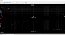
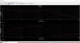
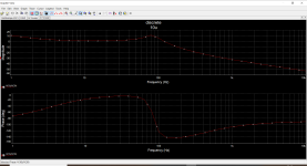
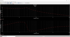
In summary, the optimal values to get good phase margin is 100n, or 1u. It actually doesn't matter THD much. Thus, I would go with 100n for now.
There are 2 poles in the bias network, C1/C2, and C5. It might be unstable! In general, we want C1/C2 to conduct for all audio frequency. Fortunately, we can play C5 a little bit to see how stable the system is.
Below is the AC sweep with different C5. The candidates are 100n, 1u, 10u, 100u.
Note: It only inspects the NFB around the bias network. Not the entire amp. Click the thumbnail below to view big pictures.


In summary, the optimal values to get good phase margin is 100n, or 1u. It actually doesn't matter THD much. Thus, I would go with 100n for now.
Last edited:
There is always something to learn.
Will it work in real life. I would say "no".
The thought experiment is as following.
Assuming upside and downside VAS have infinity Gm, and the 2 miller caps have different values, assuming 10% variant. The 10% variant will exhibit huge voltage ripple at the position of Vbe multiplier.
There are 2 possible approaches to fix that.
1. Add emitter resistors to degenerate the VAS, also add current limit mechanism to ensure VAS won't be overloaded. One of the examples is the Leach Amp. https://leachlegacy.ece.gatech.edu/lowtim/
2. Avoid Miller compensation. Without the local NFB miller caps, the output impedance of the VAS is high. There will be less hassle to join 2 high impedance nodes together. The amp still needs to be compensated by other means, most likely by shunt compensation at multiple position. One of the examples is Hafler DH-200. https://www.diyaudio.com/community/attachments/harler_dh_200-gif.70364/
Both approach would result less open loop gain. At this point, whether it performs better than a non-symmetrical topology such as Blameless is questionable.
Ah, this is a very interesting thread. I was trying to solve the same problem with my BEANS amplifier. I'll take a proper look later when I'm not falling asleep.
Overhaul the design. It can tolerant components mismatch. The NFB of the bias voltage is compensated through the conventional miller caps, too The bias voltage remains stable during clipping. Haven't verified it with TMC yet.

Clipping behavior, the bias voltage dips during clipping, I guess, because the opposite VAS runs out of current during clipping. The good sign is there is no voltage overshoot.

Clipping behavior, the bias voltage dips during clipping, I guess, because the opposite VAS runs out of current during clipping. The good sign is there is no voltage overshoot.
Last edited:
This design slightly resembles one found in the SAE MK3, designed by JB. In that design the LTP's are deliberately offset by placing high-value resistors in the feedback path -- the offset is created by the LTP bias current:PMA - Your circuit has fallen into the usual pitfall: the VAS current will vary enormously depending on the difference in offset voltage between the differential pairs.
This kind of amplifier requires that the gain of the differential pairs be kept low so that mismatched offsets do not get magnified. It is a drawback compared to amplifiers with a single differential.
Ed
-- i.e., R21-23 plus R91/92 -- which in earlier versions of the amp were replaced by a factory-selected resistor. In this design the resistors are adjusted/selected to result in a 20mA standing current in Q9 and its corresponding NPN transistor on the other half of the amplifier.
In the above screenshot I included something called a "thermal block" in the main output stage, which is a type of Vbe multiplier. It is thermally coupled to the main heat sink so it helps regulate the idle current vs. temperature. But due to temperature effects in the LTPs the circuit's performance over temperature is "complicated". The output stage is all-NPNs on the positive half, all-PNP's on the negative half of the output.
Clearly there is plenty of gain in the LTP's -- but they are made with matched devices.
I'm all-too familiar with this amp since I own one & it has a problem with one channel.
The multiple poles in the Vbe multiplier loop could well be a problem. I have experimented with some different approaches to do something similar and found that they either took a VERY long time to settle to a fixed idle current -- or went into oscillation. I have found it useful to run a simulation where the input signal goes to zero halfway through the sim, and seeing how the idle current behaves.Investigating the stability of the NFB around VBE multiplier.
There are 2 poles in the bias network, C1/C2, and C5. It might be unstable! In general, we want C1/C2 to conduct for all audio frequency. Fortunately, we can play C5 a little bit to see how stable the system is.
View attachment 1380908
Below is the AC sweep with different C5. The candidates are 100n, 1u, 10u, 100u.
Note: It only inspects the NFB around the bias network. Not the entire amp. Click the thumbnail below to view big pictures.
View attachment 1380913
View attachment 1380911
View attachment 1380912
View attachment 1380914
In summary, the optimal values to get good phase margin is 100n, or 1u. It actually doesn't matter THD much. Thus, I would go with 100n for now.
Let me explain post #16. The difference values of the mirror degen resistors deliberately creates an over-bias, but then there is a DC servo, ideally no AC feedback, that cancels any over bias up to the desired VAS current. Only one side of the VAS is sensed because the two sides are in series, so the average current is the same. You could say that the VAS is also a (DC) CCS with the feedback path through the current mirrors.
Interesting. I expect the SAE circuit to drift with temperature.This design slightly resembles one found in the SAE MK3, designed by JB. In that design the LTP's are deliberately offset by placing high-value resistors in the feedback path -- the offset is created by the LTP bias current:
Ed
Me too. I wouldn't design that way but.....there you go.Interesting. I expect the SAE circuit to drift with temperature.
Ed
- Home
- Amplifiers
- Solid State
- Symmetrical Blameless, TMC