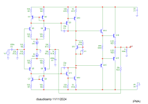
Most fully symmetrical designs have to load the input stage with resistors to define the bias for the VAS, which causes lower gain than the non-symmetric counterpart.
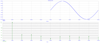
This design resolves this issue. The DC voltage of the VBE multiplier gets NFB from the input stage, so that VBE multiplier is highly regulated. As there is no fear that the bias current on VAS runs out of control, we can load the input stage with current mirror. Result higher open loop gain, and lower distortion.
PS: The simulation was run with 100mA bias at the output stage.
I would just use resistors to replace 2 current sources shown as below. As the LTP is loaded with current mirror, it has very high common mode rejection. It adds very little distortion. Creating amp is fun, creating current sources is no fun.
Last edited:
Hi @lineup
The idea is to get DC feedback from the VBE multiplier, while getting audio feedback from the output stage. It is done through C1, C2, R3, R4.
At DC, you could remove all the caps from the feedback network. Because of the nfb from the input stage, the 2 voltages at the emitters of Q1 and Q2 have to be equal. 2 VBE multipliers do their things so the bias voltage is created.
The rest of the circuit is just a symmetrical version of a Blameless amp. It is rather easy to follow.
Last edited:
Interesting idea, but I estimate the VAS current at about 2.6mA. I think R14 and R15 should be about 220 Ohms for about 10mA VAS current, better slew rate etc.
You have addressed only half of the problem. In addition to the VAS bias current needing to match, the gain of the two halves also needs to match.
Ed
Ed
The previous version may have startup issue. The input stages rely on the VBE section to provide bias, but VBE is in high impedance state when the circuit starts up. Chicken and Egg issue. I have to pull some current from outside VBE section.

I have put fixes in the OP.
I have put fixes in the OP.
Last edited:
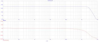
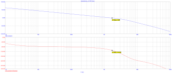
I have updated the OP adding some measurement. The R1 is a pot. Right now is at 25% of 1K, Thus, 250 Ohm. The generated voltage is about 2.4V. The bias current is about 75mA.Interesting idea, but I estimate the VAS current at about 2.6mA. I think R14 and R15 should be about 220 Ohms for about 10mA VAS current, better slew rate etc.
I probed the voltage of the VBE multiplier. Any unbalanced drive on the VAS will show up voltage ripple on the VBE multiplier. It is a valid concern. Previously, I was using 100nf (C5) on the VBE multiplier, it exhibited visible ripples. Right now, I use 100uf instead. I call it solved for now.You have addressed only half of the problem. In addition to the VAS bias current needing to match, the gain of the two halves also needs to match.
Ed
No prototype yet.I assume you have not built a prototype? Have you some results of distortion simulation? Is there any advantage of the unique Vbe multiplier and the 2 feedback points? Anyway, interesting circuit, but I would probably use a conventional Vbe multiplier and a GNFB only.
As there are two input stages loaded with current mirrors and both have tons of gain, the current at VAS is undefined. In real world, nothing is perfectly matched. A slight mismatch would results dramatical difference under gain.
2 feedback routes are used to control the voltage at the bias network.
Perhaps R3 and R4 should connect directly to C4 and C3. And PMA's circuit has ~no VAS current control.
There is another issue, ie now the output bias is largely controlled by the LTPs, so the thermal tracking is doubtful. Maybe the same idea but taken from the OP RE's would be better?
I played with the symmetric input issue and had fair results with variations on this, although I still think it's misguided.
Perhaps R3 and R4 should connect directly to C4 and C3.
Right, it also works.
Good point, Q1 and Q2 should be thermal coupled to the output transistor. Thus, they should be some things like TO-126 style so that you can mount.There is another issue, ie now the output bias is largely controlled by the LTPs, so the thermal tracking is doubtful.
Last edited:
In my email notification:
"steveu said:
Perhaps R3 and R4 should connect directly to C4 and C3.
It could work but it would also put some load on VAS. It would be less open loop gain. In the OP, the resistor is essentially bootstrapped."
Good point but why is this different than post #17 ????
"steveu said:
Perhaps R3 and R4 should connect directly to C4 and C3.
It could work but it would also put some load on VAS. It would be less open loop gain. In the OP, the resistor is essentially bootstrapped."
Good point but why is this different than post #17 ????
I realized R14, R15 put load on vas anyway on edited OP. I want to investigate more. Thus, I edited it away.It could work but it would also put some load on VAS. It would be less open loop gain. In the OP, the resistor is essentially bootstrapped."
Good point but why is this different than post #17 ????
Revised. I have updated it in OP.I realized R14, R15 put load on vas anyway on edited OP. I want to investigate more. Thus, I edited it away.
Even lower distortion.
- Home
- Amplifiers
- Solid State
- Symmetrical Blameless, TMC


