Diogo -- Answers to your questions
1. Zener voltages are given in schematic: ZD1 and ZD2 are 15V zeners.
2. Cascode stage voltage: Bases of Q4 and Q5 are held at 15v by ZD2. Voltage rail at 70V so there is 70-15V=55V drop across collectors of Q4 and Q5.
3. Current through cascode: Look at the constant current source biasing the differential pair at input. ZD1 holds base of Q1 at 15V. There is a 15 - 0.6 (Q1 base-emitter voltage)= 14.4V drop across R8 (10K ohm. So current through Q1 is 1.4mA, or 0.7mA through Q2 and Q4 and the remaining 0.7 mA through Q3 and Q5.
These are approximate calculations but good enough.
R6 takes up some voltage but also the capacitance is reduced 18k//1-4pF instead of the Ccb of Q1 which is more (haven't checked the datasheets) I think.
I have wondered myself if this resistor is good or bad if we talk frequency response properties of the current mirror.
I have wondered myself if this resistor is good or bad if we talk frequency response properties of the current mirror.
peranders said:R6 takes up some voltage but also the capacitance is reduced 18k//1-4pF instead of the Ccb of Q1 which is more (haven't checked the datasheets) I think.
I have wondered myself if this resistor is good or bad if we talk frequency response properties of the current mirror.
Interesting point, but I have one immediate objection. Don't we
just push the problem down to Q1 anyway? Since the current
through R6 is almost constant, the voltage over R6 will be
almost constant. Hence the the collector voltage of Q1 will still
have to follow the common point of the degeneration resistors
(but level shifted) just as it would without R6. It seems to me
that Ccb of Q1 would still have the same influence, assuming
it is considerably larger than the parallel capacitance of R6.
Maybe I make some error in this reasoning, but I am sure you
will point it out in that case.
otherwise, I am a bit puzzled by the use of R6. The obvious
explanation would be to reduce Vce of Q1, but I see not
reason for this, since it is rated 300V 20W.
Per and Christer - I hear you. I've seen other schematics with this resistor and usually end up scratching my head about its presence.
For a few pennies more, he could have used a cascode current source and gotten a real improvement.
For a few pennies more, he could have used a cascode current source and gotten a real improvement.
cascode
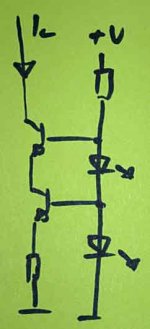
Shouldn't the base of the lower transistor be unconnected (input) and the base of the upper transistor be biased with the resistor upwards and the two diodes/LEDs downwards?
Carlos
Shouldn't the base of the lower transistor be unconnected (input) and the base of the upper transistor be biased with the resistor upwards and the two diodes/LEDs downwards?
Carlos
NOTE: My sketch was a current source, not a gain stage. (No input signal!)
The lower transistor determines the current. The upper transistor fixes a constant voltage across the collector-emitter of the lower transistor. If you for an example have a power amp with +-70-100 Volts, the upper transistor will be a 200-300 Volt type and the lower one is a BC5xx type with 30-70 V Vce. In this case the base of the upper transistor will be 15-20 volt over the most negative voltage (ground in my sketch). The upper transistor "isolates" the lower transistor from high voltage, also the current source will get high output impedance, very positive side effect.
The lower transistor determines the current. The upper transistor fixes a constant voltage across the collector-emitter of the lower transistor. If you for an example have a power amp with +-70-100 Volts, the upper transistor will be a 200-300 Volt type and the lower one is a BC5xx type with 30-70 V Vce. In this case the base of the upper transistor will be 15-20 volt over the most negative voltage (ground in my sketch). The upper transistor "isolates" the lower transistor from high voltage, also the current source will get high output impedance, very positive side effect.
- Status
- Not open for further replies.
- Home
- Amplifiers
- Solid State
- Symmetrical 400W amplifier