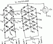
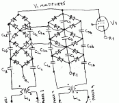
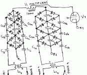
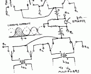
Here is a new way to do output transformer impedance conversion without using a transformer. This uses a switched capacitor converter or voltage multiplier using typically Mosfets for switching. Two converters are needed to power the speaker in both polarities.
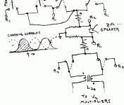
The attached diagram(s) shows one of them in simplified form. Four switching phases per converter are needed to perform ripple free impedance conversion using the resonant charging inductors shown as L1a and L1b. The resonant charging allows the switches to operate during times with zero voltage across them, thus avoiding generation of EMI. Charging currents are then two 180 deg. sine wave phases summing to a constant current. (see graph)
Signal ground for the tube drives is placed at the center of the speaker effectively, so this is like having the usual secondary winding act as a CT (center tapped) CFB (cathode feedback) winding for the tubes. This places half the low voltage speaker voltage in CFB for each tube, so is still easy to drive.
Charging current thru one single phase of the multiplier is shown in the graphic by cross lines on the current waveform. The other second phase does the next continuous cycle. And the other two phase converter section provides the dashed charge current waveform. Both two phase converter sections then combine to give ripple free smooth charge transfer for one tube.
The V2 tube multipliers, not fully shown at the bottom, handle the other tube V2 for Push-Pull operation.
Similar in concept to the Berning impedance converter, the Switched Capacitor Convertor also provides the HV for the tubes operation by conversion of the LV supplies to HV at the tube anodes.
Capacitors are of course quite small values here, in the pFs, this must be so as to provide adequate audio bandwidth (the tube sees them in series connection shunting its output). The high switching frequency then lowers their impedance for the carrier sine waves, so as to tranfer the large currents at the speaker end of the multipliers.
Don
Couldn't get the full diagram to post, so I split it in two pieces.
Attachments
and the other half:
The number of capacitors stacked up in the multipliers can of course be increased for higher "turns ratios". Ie, 10 caps stacked up give 10 to 1 turns ratio, or 100 to 1 impedance ratio.
(I just bought some stock in diode manufacturers, seeing as how many they will have to sell for this! 😀 )
Don B.
The number of capacitors stacked up in the multipliers can of course be increased for higher "turns ratios". Ie, 10 caps stacked up give 10 to 1 turns ratio, or 100 to 1 impedance ratio.
(I just bought some stock in diode manufacturers, seeing as how many they will have to sell for this! 😀 )
Don B.
Attachments
Error fix in diagram:
The diagram has one too many diodes in the multiplier stacks. The bottom diodes (to the R1 connection and L1 inductors) are not needed. Corrected diagram (top part) attached.
Just for laughs, I calculated the number of diodes needed to build one of these OTLs. For an N to 1 turns ratio (N*N impedance ratio) one needs 16N diodes and 12N caps. So for a 10 to 1 turns xfmr, you'll need 160 diodes and 120 caps. Well, quantity discounts kick in at that level at least. Obviously need a PC board for this design.
Don
Attachments
Optimiziations, fixes
The previous diagrams attempt to economize on capacitors by replacing the central stack caps on the left section by cross links to the right section. I'm not sure this is working correctly without causing interference between the resonant operation in each stack. (needs to be simulated or experimentally checked)
So I have attached a new diagram without this economizing. The two stacks operate independantly here, with the center tapped ripple inductor at the top combining the two outputs to provide ripple free voltage for the tube. This inductor is relatively small, only handling ripple. It will have a hardly any influence on the overall resonance frequency of operation since it is acting as a balun xfmr with matched opposite ripple voltages on each side.
I have attached a new diagram again, with these amends.
Optimizations:
Usually, these V multiplier stack circuits are presented using identical capacitors everywhere. But for handling power, and bandwidth optimization, some improvements can be made I think.
Since current increases toward the speaker (& Mosfets) end, the caps should be bigger there. (Also, the diode current ratings too)
So start with X pF's at the top stack capacitors and increase by N as approaching the bottom. (ie, 1X, 2X, 3X, 4X, ..... ) This goes for both central caps and the side transfer caps.
The result will be N fold better current handling at the speaker end while only doubling shunt capacitance seen by the tube. There could be some optimization of relative capacitance between the central stack and transfer caps too, not sure yet, but I would expect the central ones might be 2X bigger, using 2 phases per stack. (needs testing)
Maybe the just added CT ripple inductor can be deleted without much effect, requires testing.
Diodes need to be able to handle a minimum of 2X the low voltage supply.
Don
Attachments
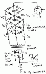
Bottom part of the diagram again:
Notes: The Mosfet switches operate as 180 degree conducting pairs on each stack, with the left stack 90 degrees shifted with respect to the right stack. Hence the phases are shown as phase 1,2,3,4 with 90 degrees between each one.
The battery symbols are the low voltage supplies, they provide the peak speaker voltage required PLUS 1/N transformed minimum operation voltage of the tubes. Ie, if the tubes require 100 V at maximum current, then 100/N volts are needed besides (ie, plus)the peak speaker voltage at the LV supplies (plus a bit more for diode drops etc.).
Don
Attachments
Switched LC Converter
Next up, I have combined the switched cap. converter and the switched inductor converter to gain some part count optimization.
This now requires half as many Mosfet switches (8 instead of the 16 for the Sw cap. conv.). The "turns ratio" will now be the product of the M:1 turns ratio inductor and the N:1 capacitor stack multiplier. This saves on capacitor and diode count considerably, while still using the same number of inductors. (The M:1 inductor here, and the previous L1a ... inductors, are all air gapped inductors for resonating with the caps.)
We also avoid the need for full HV windings on the xfmr/inductors due to the cap. multiplier sections, which improves windability, reliability, and reduces distributed shunt capacitance in the HF xfmr.
The isolation afforded by the secondary windings on the M:1 inductors now allow us to dispense with the CFB arrangement if desired. (one can still do the CFB approach if wanted). So the speaker gets one side grounded, instead of the circlotron like arrangement used before in the Sw Cap. Conv.
All Mosfets have their source terminals grounded now, for easier drive signal connection. (The Mosfets still require snubber networks across the drain - source terminals for protection from inductive transients when turning off. All switched conv. versions require this, I just left it out of the diagrams for simplification.)
The use of four phases, like before, (only one conv. stack shown in the present diagram) means we operate without ripple in the currents or voltages. The resonant operation mode allows zero current switching to avoid EMI or losses like before.
And finally, the use of a voltage multiplier section provides maximum current limiting in the event of shorted speaker terminals or tube arc-over.
I should also note that the full wave, 90 degree overlapped operation, used in these designs means continuous ripple free current conduction.
HV multiplier circuits usually are associated with drooping voltages when loaded down. This is because of their usual implimentation as discontinuous conduction, high ripple designs.
Not here! (or the previous Sw Cap. Conv.) You will find that these continuous conduction converters can have VERY low internal resistance. (WARNING! Do NOT put your hands across the high voltage! It won't sag a bit here.)
Don
Attachments
- Status
- Not open for further replies.