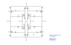
Please find attached a proposed schematic [jpeg and pdf] describing the subject title. I will explain its operation in a future post; unless someone else beats me to it. Please look at the picture and note:
- Two F5s are shown.
- The right side amp is hand-drawn and is skeletal. It is a mirror image of the left side side amp. The right side amp amplifies the Negative input signal.
- The schematic of the left side amp is well-known to y'all. I whited out some of the bias elements around the power output P-MOSFET for the sake of clarity. It amplifies the Positive input signal.
- Note the resistor Rxt which cross-couples or joins the source ports of the power output P-MOSFETs Q3 and Q3'.
- Ditto for the resistor Rxb which joins [cross-couples] the source ports of the output power N-MOSFETs Q4 and Q4'
Attachments
![SuSy[R]balF5.jpg](/community/data/attachments/322/322230-201805b4bf4a871ea1b65b777e31b101.jpg?hash=IBgFtL9Khx)
without even going in analysis of drawn sch further , to examine is it SUSY or not - establishing SUSY mechanismus on output is waste of electricity , if not quality
without even going in analysis of drawn sch further , to examine is it SUSY or not - establishing SUSY mechanismus on output is waste of electricity , if not quality
Zen Mod; patience my dear man. The following questions hang:
- Does balanced F5 need SuSy?
- Will SuSy improve the already excellent performance of balanced F5?
- What is the mechanism which explains how it works?
- What is the value of Rxt and Rxb [cross-coupling resistors] which give the least amount of net distortion?
- Should both channels be highly matched?
- Signal flows from encircled point #1 to encircled point #2 which is the source port of Q3.
- Since the sine waves are 180 degrees out of phase and have identical peak to peak amplitudes [matched amps], they add up by superpostion to wipe out/cancel each other.; but they leave behind the distortion arrow pointing up.
- Q3 [of left amp] operates as a common gate amplifier to the residual arrow signal.
- The arrow signal appears at the drain of Q3 [encircled #3] while retaining its parent phase [still pointing up]
- The left amp then proceeds to wipe out/cancel the distortion arrow via its overall Pass negative feedback as follows.
- Let us follow the path of the distortion arrow signal which reaches the source port of 2SJ74 [encircled #4]
- The JFET treats this signal arrow by operating in the common gate configuration.
- The signal arrow emerges at the drain of 2SJ74 [point #5] while retaining its parent phase [still pointing up]
- The signal arrow is fed next to the gate of Q4. The source port [encircled #6 ] retains the phase of the parent distortion signal arrow [still points up]. This encircle point #6 is the important signal for this current SuSy [R]. By contrast, Q4 inverts the phase of the distortion signal arrow at its drain port [encircled #7]. The distortion arrow at # 7 poind down and thus wipes out the instigating distortion arrow pointing up at #3. There is no net distortion arrow at the Positive power output port.
- Let's examine the distortion arrow signal [pointing up] at encircled point#6 [source port of Q4]
- It reaches the source port of of Q4' via the cross-coupling resistor Rxb.
- Q4' operates in common gate configuration. So the distortion arrow points up and rides with the half shaded portion of its power output signal at encircled point #8.
- But, the distortion arrow signals at the source and drain ports of Q3' [right amp P-MOSFET] are inherently out phase. The music signal at the drain of Q3' has its distortion arrow pointing down while the music signal at the drain of Q4' [in phase with the former one] has its signal distortion arrow 180 degrees out of phase [pointing up].
- We have a desired situation of distortion wipe-out or cancellation.
- The Negative power output port is void of distortion.
- Thus, the power signal flowing through Zload is pristine.
Seems like you are attempting to "cross couple" a bridged version of the F5...??
Perhaps you might start with Evul's F5X, as a starting point?
Distortion cancellation between the two "sides" may not really be possible by the means you are thinking about. Even if you get "distortion cancellation" you may find that you've knocked out the very nice even order stuff and left some nasties in odd higher order stuff, perhaps.
Just some random thoughts.
Your next step is to simulate it in LTSpice, and see what these connections actually do. To start you can use generic spice models for the parts. Once you get some improvement, and the improvement is reasonable, then get better models. Finally, breadboard the circuit and see if it really works.
_-_-
Seems like you are attempting to "cross couple" a bridged version of the F5...??
Perhaps you might start with Evul's F5X, as a starting point?
Distortion cancellation between the two "sides" may not really be possible by the means you are thinking about. Even if you get "distortion cancellation" you may find that you've knocked out the very nice even order stuff and left some nasties in odd higher order stuff, perhaps.
Just some random thoughts.
Your next step is to simulate it in LTSpice, and see what these connections actually do. To start you can use generic spice models for the parts. Once you get some improvement, and the improvement is reasonable, then get better models. Finally, breadboard the circuit and see if it really works.
_-_-
Thank you bear for your thoughts.
- Yes the schematic in Post #1 cross couples two F5s operating in a bridge or balanced or differential manner.
- The schematic of F5x is not published. EUVL's approach is not known for comparison.
- US 5,376,899 [Pass] teaches a method to lower the %THD of audio power amps to even lower values. F5 has an impressive low %THD to begin with; which in this balanced configuration can be lowered even further.
- In addition to your recommendation of using LTSpice, a DIYer who already has a stereo F5 may wish to do the experiment. Only two power resistors are needed to generate a monoblock. I do not know their values; but there is an answer.
Looks like you have not bothered to read the F5x Threads.......[*]The schematic of F5x is not published. EUVL's approach is not known for comparison........
Thanks AndrewT. Please point me to the postLooks like you have not bothered to read the F5x Threads.
NB. The post is #167 in F5x ..The EUVL Approach .. Builder's Thead.
Last edited:
Antoinel , you're attaching trailer to dragster , hoping that it will be more stable and twice faster , in same time
however - SUSY is feedback based thing ; what you're intending is completely different ;
fact that's ineffective is of secondary importance
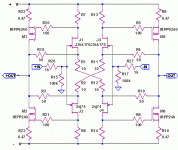
here's early EUVL's F5X ; there must be more readable schematics buried in the thread and maybe on EUVL's site
as you can see - solution is simple , effective and elegant
there are few other solutions to make bridged F5 SUSY , this one is published and covered as project for 158%
however - SUSY is feedback based thing ; what you're intending is completely different ;
fact that's ineffective is of secondary importance
here's early EUVL's F5X ; there must be more readable schematics buried in the thread and maybe on EUVL's site
as you can see - solution is simple , effective and elegant
there are few other solutions to make bridged F5 SUSY , this one is published and covered as project for 158%
Attachments
Last edited:
Antoinel , you're attaching trailer to dragster , hoping that it will be more stable and twice faster , in same time
however - SUSY is feedback based thing ; what you're intending is completely different ;
fact that's ineffective is of secondary importance
here's early EUVL's F5X ; there must be more readable schematics buried in the thread and maybe on EUVL's site
as you can see - solution is simple , effective and elegant
there are few other solutions to make bridged F5 SUSY , this one is published and covered as project for 158%
Thanks Zen Mod for the schematic, and your valuable comments leading to the following:
- You know the published work of Mr. Pass like the back of your hand. I'll take your word to heart that my schematic in post #1 is not SuSy [R]. Thus, I apologize to Mr. Pass for wrongly using Super Symmetric [R] in the title, and SuSy [R] in this post.and the above. It follows that from this point forward ,I will not use the aforementionned words; and not reference US 5,376,899 either. It also follows that the new title of this thread is "A cross-coupled pair of F5s". It is a much better fit.
- Experiments will determine whether this style of cross-coupling [post #1] affects the net performance of the bridge amp. You surprised me when you declared this approach to be ineffective.
Or, I'll start a new thread which is entitled "A cross-coupled pair of F5s". I declare this current thread dead and obsolete ; meaning I will refrain from posting anything else in it.
Last edited:
In EUVL's threads you can find many informations about this topic, some possible designs how to bridge and the reasons for their final solution. There's also a build thread, very excellent documented. (If I knew where all this info were, I'd have postet the links here).
Kind regards,
Matthias
Kind regards,
Matthias
Antoinel, sometimes to get things done you need to maintain radio silence from diyA...then it's time to start a thread when you have results to share 🙂

- Status
- Not open for further replies.
- Home
- Amplifiers
- Pass Labs
- Super Symmetric [R] Balanced F5