Thank you Jan this suggestion is very helpful!!
Since this is my first real diy project I really appreciate your help and guidance.
I will prepare a new schematic (based on # 601) and an image of the wiring and grounding.
Michael
On 601, ONLY move the pot bottom from power supply ground to some point on the board maybe call it 'signal return' and that is the bottom of C103/103, maybe call it agnd.
Don't continue to change all these labels, it's impossible to keep track.
Jan
It would be nice and helpful to see a photo of the H/amp PCB and a labeled diagram of the same pcb with all the pins in the correct locations.
Then use that pic in all subsequent postings.
Then use that pic in all subsequent postings.
post610 and 616 have lost the Power Ground (PSU Zero Volts) pin/pad.
Why did you remove it?
Go back to 601 and add on all the in/out pins/pads.
Why did you remove it?
Go back to 601 and add on all the in/out pins/pads.
Wouldn't it be better to have the DC blocking capacitor AFTER the pot wiper, before the input resistor?
That leaves the source to run a little 'wetting' current across the pot wiper contacts. Unless the source has its own DC blocking, in which case, do you need another DC blocking? My experience is that DC blocking capacitors have an adverse effect on the sound quality and I never use them.
One can understand their use in low cost consumer electronics made to a poor tolerance. But this is (supposed to be?) bespoke high quality tight tolerance where DC offset can be minimised by the design and the component selection.
And shouldn't the Super Reg ground sense be connected to the amplifiers AGnd rather than the power supply earth star?
Might you be better off not using a three pin headphone connector with combined earths, but instead a four pin XLR, or two three pin XLR (do they make two pin?), so as to continue the speakers earth return back separately, as there is current there and you don't want to cause some small voltages across the connectors that affect the other channel? Of course that is nullified if you're using a combined earth wire from the speakers. I use two separate pairs all the way back to the amplifiers (which at the moment are 'balanced', so no earth return). With my loud speaker power amplifiers I take the earth return from the speaker direct to the PSU caps earth star, it was a large improvement in every way vs. terminals to wire to tracks to more wires to a common point somewhere. And the thicker the earth plate or rod, joining the PSU caps ground, the better the sound quality (transient response, clarity, etc).
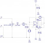
Ok please find attached the latest changes. Vin- is agnd the bottom of C103/R103. C101 has been moved after the pot.On 601, ONLY move the pot bottom from power supply ground to some point on the board maybe call it 'signal return' and that is the bottom of C103/103, maybe call it agnd.
There is still a remaining question: Is there a connection to the chassis except the pot's metal body?
Michael
Attachments
I think this should do it.
Indeed you'd want to connect the whole system to the chassis somewhere. One thing you can do is connect each power supply GND to chassis through a 10 ohms resistor. Low enough to connect, high enough to keep out any residual currents.
For RF suppression you could bridge this resistor with say 1000pF.
Jan
I think this should do it.
Thank you all for your help🙂
Do you mean 4xSuperRegulator GND?Indeed you'd want to connect the whole system to the chassis somewhere. One thing you can do is connect each power supply GND to chassis through a 10 ohms resistor. Low enough to connect, high enough to keep out any residual currents.
For RF suppression you could bridge this resistor with say 1000pF.
I have read about using a resistor and a capacitor as 'ground breaker' to connect mains earth (220V AC) and dc GND. Why do I have to use a 'ground breaker' in a completely isolated chassis?
Michael
look at the resistances (DC impedances) fed into the +IN and -IN of the opamp.
One is infinite and the other is <680r
Even a jFET input stage will not like this and output offset will be a symptom.
One is infinite and the other is <680r
Even a jFET input stage will not like this and output offset will be a symptom.
Are the 6 labeled pads/pins all that the H/amp PCB has for in/out?
Are there any others?
The Headphone output socket is still connected to the PSU zero volts. Break this connection on both channels.
Instead find the signal return from the headphone back into the H/amp PCB.
You may find that the Power Ground is trace connected to one of the in/out at the other end. Or connected via a lowish value resistor.
You may find that Vin- is a likely candidate.
Hi Andrew,Are the 6 labeled pads/pins all that the H/amp PCB has for in/out?
Are there any others?
The Headphone output socket is still connected to the PSU zero volts. Break this connection on both channels.
Instead find the signal return from the headphone back into the H/amp PCB.
You may find that the Power Ground is trace connected to one of the in/out at the other end. Or connected via a lowish value resistor.
You may find that Vin- is a likely candidate.
thank you for your comments. Please be patient with me I am a real beginner.
My understanding so far:
At a certain point the PSU zero volts must be connected to the amps GND. Furthermore, I got two GNDs or INs- from the signal source via the RCAs. So this adds up to four different GNDs.
Then the question is where to connect all these GNDs?
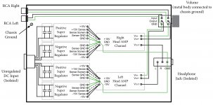
This is why I have drawn a new image #616 to create a star ground connecting all the GNDs (4 Superregs, RCA left and right, amp left and right, headphone jack).
Michael
Last edited:
Please correct me I'm wrong but...
With output stages, such as a headphone driver, there is current, not only voltage.
You have to consider the full current path. Where is coming from? Pin 6 of the op-amp. But how does it get to there? From pins 4 and 7.
There's no local capacitance at the op-amp to deliver current so it's getting to pins 4 and 7 from the outputs of the two super regulators output transistors (as the caps there are for stability, not current delivery?).
Before those, it comes from ONE PLATE of each rail of the main capacitors (having been charged up by the transformer).
So the current has to return to: THE OTHER PLATE of each rail of the main capacitors, which in this case would be their earth star. That is the full current path.
Eg, main Cap +ve plate, regulator, amplifier, load, main cap -ve plate.
As the electrons flow out of one side of the main capacitor to the load, an equal amount of electrons flow into the other side of the main capacitor from the load. Or the speaker won't move.
Alternating with the opposite for the other rail.
I don't know if this regulator design 'expects' the return current to travel via it's ground rail and compensates for any slight voltage changes caused by it's passing, in which case the ground and ground sense joint would be the correct place to return the current? Perhaps Jan can answer this? 🙂
Last edited:
Hi all. I am searching for the Q2 transistor and having a bit of trouble. Are these BC556BP available anywhere?
Thanks!!
Thanks!!
You can use BC557, 558, 558 560 B and C model. The only thing you must be aware of is the collector emitter voltage. I'll guess you will have less than 30 volts in so it won't be a problem.
so is it post616 with 9in/out, or post625 with 6in/out, that shows the PCB pins/pads?........................
This is why I have drawn a new image #616 to create a star ground connecting all the GNDs (4 Superregs, RCA left and right, amp left and right, headphone jack).
Michael
Show a photo and label up a diagram to match exactly.
It would be nice and helpful to see a photo of the H/amp PCB and a labeled diagram of the same pcb with all the pins in the correct locations.
Then use that pic in all subsequent postings.
Last edited:
Please correct me I'm wrong but...
With output stages, such as a headphone driver, there is current, not only voltage.
You have to consider the full current path. Where is coming from? Pin 6 of the op-amp. But how does it get to there? From pins 4 and 7.
There's no local capacitance at the op-amp to deliver current so it's getting to pins 4 and 7 from the outputs of the two super regulators output transistors (as the caps there are for stability, not current delivery?).
Before those, it comes from ONE PLATE of each rail of the main capacitors (having been charged up by the transformer).
So the current has to return to: THE OTHER PLATE of each rail of the main capacitors, which in this case would be their earth star. That is the full current path.
Eg, main Cap +ve plate, regulator, amplifier, load, main cap -ve plate.
As the electrons flow out of one side of the main capacitor to the load, an equal amount of electrons flow into the other side of the main capacitor from the load. Or the speaker won't move.
Alternating with the opposite for the other rail.
I don't know if this regulator design 'expects' the return current to travel via it's ground rail and compensates for any slight voltage changes caused by it's passing, in which case the ground and ground sense joint would be the correct place to return the current? Perhaps Jan can answer this? 🙂
Your reasoning is correct, what goes out must come back ;-)
I's a very well known law: at each circuit node, the sum of currents going in and out is always exactly zero. Just as the voltages, going around in a loop, always add up to exactly zero 🙂
OK, off the soapbox.
Look at the regulator as 'modulating' it's 'resistance' such that whatever the currents in any branch of the circuits at a certain moment, the resulting voltage across the load is precisely controlled.
The reason for remote sensing is exactly to make sure that what is controlled is the voltage at the load.
Jan
Hello,
When will the 2.3 ver of the super regulator boards be in stock??
I send all files to Jason, I think he ordered the boards.
Jan
Hi all. I am searching for the Q2 transistor and having a bit of trouble. Are these BC556BP available anywhere?
Thanks!!
Yes, any small signal transistor with the voltage rating and Hfe>100 will do.
BC5xx are CBE
Try to find CBE device, or EBC device, as an alternative.
But do record whether you have used EBC or CBE.
It is critical to assembly and to debugging that your know if the device needs to be reversed at insertion.
Try to find CBE device, or EBC device, as an alternative.
But do record whether you have used EBC or CBE.
It is critical to assembly and to debugging that your know if the device needs to be reversed at insertion.
- Home
- The diyAudio Store
- Super Regulator