I almost killed mine when I followed the service manual. Luckily I was using a dim bulb tester. I know more people who have had the same issue due to the faulty service manual. Maybe some examples have been corrected, such as yours.
Figure 3-1 in the service manual is correct for F-2580 driver board? According to the paper service manual I have and the downloadable ones as well. Maybe its different for the F2583 driver boards that go with the F-2582 driver board power supply?
Is the bulb of the limiter contiuing to glow after settling? If only faintly, it's probably reasonable to test without it now, and check those voltages again. They will vary with bias level and probably according to predriver and driver transitor Beta, since the 1k base resistors R37,38 mean the whole bias spreader arrangement is unbalanced until the correct current is set, I guess.
There is a nominal 2V rail offset, so I'm not sure what difference there should be, if any, between those bias voltages.
Vbias of the driver and output stages should be around 4 x diode drops or ~2.6V total. You have ~ 2.3 and 2.7 which isn't so bad even if unenevenly spread. I think there is still a problem there, perhaps as you do. Hopefully reoldering will find it, assuming all the semis are still fine by Vbe checks etc.
Soldering failures are still dogging you and they'll continue to, until you systematically reflow them on the power amplifier boards at least. Inspection by microscope might be interesting but until all joints are reflowed, you can't be certain you have found them all. It might sound like a chore but it's got to be quicker and less agony than finding them one by one 😉
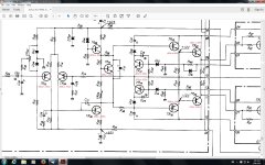
Ive resoldered the whole driver board and set the bias to 25ma and 26ma thats as far as they go then I set the DC offset on the left to under 1mv then I tried the right channel which was 600mv,I got it down to 120mv and smoke started coming from the driver board,the bulb only lit up a bit though. I found R54 68 ohm resistor had burnt a bit and everything else was OK I went over some more solder joints just in case and tried again I reset the DC so that both sides were under 1mv then connected up a DMM on both channels to do the bias and just after I turned it on the bulb went full on bright. I quickly turned it off and unplugged the power to the driver board then turned it back on,I tested the voltages on the power supply F-2567 and they all appeared to be OK! So its still on the driver board somewhere but I cant work it out ? Ive taken both of the output transistor modules apart and resoldered everything including the big capacitor power supply. Well at least its narrowing it down but Im wary of giving it full power because there must be an intermittent short somewhere on that driver board? Ive gone over every inch with a magnifying glass and running a fine jewlers screw driver around the solder joints to clean off any stray solder etc...Ive put the driver board Collector and Emitter readings on the schematic,they read OK to me? This is starting to become a pain and Im a very patient person as a rule.lol 😀 PS I nearly forgot to say I was getting 40 plus volts on the output Power module emmitter resistors every now and then?
Attachments
Last edited:
I've been working on a damn Sansui AU-11000 Amp, Replaced ALL 8 of the Power Transistors with OnSemi MJ21193's & MJ21194's, and ALL the Capacitors on the Bias Board.
The Bias Board has the VR-Trims Labeled DIFFERENTLY compared to the Diagram in the Service Manual. So, I Figured I'd turn the VR03 & VR04 [Whatever the hell they are now...] All the way Clock-Wise as stated in the Manual. But Basically, that means VR01 & VR02 according to the Service Manual. Well.... The damn thing over-heated in about 5 Minutes warming it up, and it wasn't but a couple of minutes into 'Theoretically' Adjusting the DC-Offset that the Power-Light went Red, which is Protection Mode to my understanding.
I've been working on Computers & Electronics for over 12 Years, and I can't even figure out how to Properly Adjust the DC-Offset much less the Current-Bias!!
No One can tell me where VR01/VR02 are even Located, as the Manual COULD be wrong, and the Board could ALSO be wrong!!
[The F-2583 has the VR01 & VR02 Labeled where VR03 & VR04 are shown in the Service Manual]
I'm Seriously Fed-Up with this damn Sansui Amp.
If Anyone has a CLUE on how to Instruct me on how to PROPERLY Adjust the DC-Offset & Bias-Current, I'd be more than Happy to Listen. Until then, I am DONE with this Amp.
I thought you had it sorted out with that corrected diagram for the F-2583 bias and DC offset? You could check that your posistors are working OK for thermal runaway!(broken wire maybe?) Check the regulator/protection board components,the 5w resistors there get really hot make sure that board is plugged in properly and the bracket that holds it in is tight. Im having the same problem as you basicly.Ive been at this same problem for about 2 months. I just came back from a break just so I wouldnt go crazy. lolI've been working on a damn Sansui AU-11000 Amp, Replaced ALL 8 of the Power Transistors with OnSemi MJ21193's & MJ21194's, and ALL the Capacitors on the Bias Board.
The Bias Board has the VR-Trims Labeled DIFFERENTLY compared to the Diagram in the Service Manual. So, I Figured I'd turn the VR03 & VR04 [Whatever the hell they are now...] All the way Clock-Wise as stated in the Manual. But Basically, that means VR01 & VR02 according to the Service Manual. Well.... The damn thing over-heated in about 5 Minutes warming it up, and it wasn't but a couple of minutes into 'Theoretically' Adjusting the DC-Offset that the Power-Light went Red, which is Protection Mode to my understanding.
I've been working on Computers & Electronics for over 12 Years, and I can't even figure out how to Properly Adjust the DC-Offset much less the Current-Bias!!
No One can tell me where VR01/VR02 are even Located, as the Manual COULD be wrong, and the Board could ALSO be wrong!!
[The F-2583 has the VR01 & VR02 Labeled where VR03 & VR04 are shown in the Service Manual]
I'm Seriously Fed-Up with this damn Sansui Amp.
If Anyone has a CLUE on how to Instruct me on how to PROPERLY Adjust the DC-Offset & Bias-Current, I'd be more than Happy to Listen. Until then, I am DONE with this Amp.
Last edited:
Redrooster - I've found the TR07 & TR08 to have No Continuity at the Emitters. They are supposed to one-way, like a Diode. I think this is the Issue. I know I'm testing these things in the Circuit, but there should be a sign of Some Continuity at the Emitter with my MultiMeter Leads one way or the other. It seems my experience with Computers isn't very helpful on Vintage Audio Amplifiers. Or HDTV's for that matter 😛
Perhaps junking these things for NEW Amps makes allot more sense. You could spend $1200+ and hundreds of hours trying to make these Vintage Amps work like the day they were new, and they still aren't worth it. If this was how Computers were, we would be using Technology from the Early-90's, and the Pentium 386 would be around the Corner.
It would be like hiring a Paramedic-Team to work on one, too. Thus, it would be like it was then: 1 in 20 people own a Computer. It's also amazing how the Service Manual doesn't even mention issues with over-heating the Amp, which is 3 Circuit-Boards.
I'm Embarrassed to have had this much trouble working on a Circuit Board I've diagnosed Twice, only to find I can't find a simple (but specific) PNP Transistor.
Live and learn mate.lol These vintage amps can be frustrating to say the least.Recheck the pinouts on TR07/08? Its so easy to get them mixed up,theres a set of diagrams on page 15 of the sevice manual that shows them.That could be the problem by the sounds of it? TR07/08 are in your constant current circuit.Redrooster - I've found the TR07 & TR08 to have No Continuity at the Emitters. They are supposed to one-way, like a Diode. I think this is the Issue. I know I'm testing these things in the Circuit, but there should be a sign of Some Continuity at the Emitter with my MultiMeter Leads one way or the other. It seems my experience with Computers isn't very helpful on Vintage Audio Amplifiers. Or HDTV's for that matter 😛
Perhaps junking these things for NEW Amps makes allot more sense. You could spend $1200+ and hundreds of hours trying to make these Vintage Amps work like the day they were new, and they still aren't worth it. If this was how Computers were, we would be using Technology from the Early-90's, and the Pentium 386 would be around the Corner.
It would be like hiring a Paramedic-Team to work on one, too. Thus, it would be like it was then: 1 in 20 people own a Computer. It's also amazing how the Service Manual doesn't even mention issues with over-heating the Amp, which is 3 Circuit-Boards.
I'm Embarrassed to have had this much trouble working on a Circuit Board I've diagnosed Twice, only to find I can't find a simple (but specific) PNP Transistor.
Last edited:
I'm not sure what you mean, Redrooster.
There are only 3 Pins on a Transistor, and the Board has the Collector, Base and Emitter labeled by the Pins Holes in the Board. I found that the Base & Collector are working as expected with one another, but nothing from the Emitter using my Multimeter.
These are all Originals, and don't appear to have been removed. They are also consistent with other pictures I've seen of the F-2583. If I had known these were bad, I would have replaced them. But I assumed that 'Funny Readings' were OK in the Circuit. But that's not a good assumption... The Emitters should have showed Something one-way or the other on the Multimeter. All the other Transistors did. I know that some have the Emitter in the Center (Pin 2), and some have the Emitter on one of the Sides.
Thanks for the Advice! 🙂
Check the battery in your DMM,you just never know The original transistors are known to fail with age.
Last edited:
Here is the Pin Order (Pin Out) of the A818's according to the labeled pins on the F-2583 Board:
1: E
2: B
3: Not Labeled [C]
I looked up the 2SA914, and it's got the Collector in the Center (Pin 2) and Base on the Side (Pin 3). I'm not sure if it's a good idea to use Transistors with different Pin-Orders.
1: E
2: B
3: Not Labeled [C]
I looked up the 2SA914, and it's got the Collector in the Center (Pin 2) and Base on the Side (Pin 3). I'm not sure if it's a good idea to use Transistors with different Pin-Orders.
Here is the Pin Order (Pin Out) of the A818's according to the labeled pins on the F-2583 Board:
1: E
2: B
3: Not Labeled [C]
I looked up the 2SA914, and it's got the Collector in the Center (Pin 2) and Base on the Side (Pin 3). I'm not sure if it's a good idea to use Transistors with different Pin-Orders.
What else are you going to use? They are the replacements so youre going to have to get the pinouts right.Everyone else has no problem with it! If your 2SA818s are no good then order the 2SA914s and 2SC1953s. You may as well use MJE15030/31s for your driver amplifiers going to the output module as well because the original transistors will fail.Get 4 T0-202 MJE15030s and 4 MJE15031s replace the first two rows of transistors with them.Swap NPN for NPN,PNP for PNP. The PNPs will need to face backwards on the second row.Put some heatshrink on the center pin to stop any shorting when you cross the pins over.
A long time ago, I found a problem on two different Sansui products :
resistors of the power supply decoupling circuit (R58 and R60 in the figure) had gone wrong with the time, they became of much higher value without apparent signs of degradation.
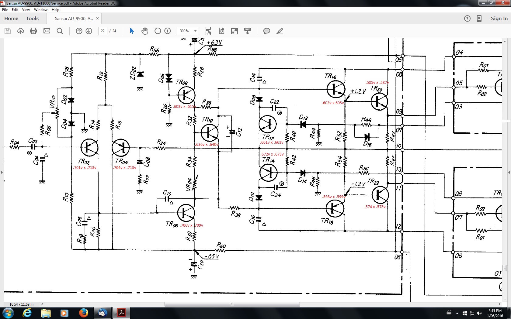
resistors of the power supply decoupling circuit (R58 and R60 in the figure) had gone wrong with the time, they became of much higher value without apparent signs of degradation.
A long time ago, I found a problem on two different Sansui products :
resistors of the power supply decoupling circuit (R58 and R60 in the figure) had gone wrong with the time, they became of much higher value without apparent signs of degradation.
I had the same problem on my driver board years ago they are 220 ohms mine read 1800 ohms.lol
- Status
- Not open for further replies.
- Home
- Amplifiers
- Solid State
- Strange Sansui Driver Board Problem?