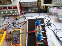
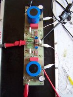
I had made F5 boards a couple of years ago but never followed up this project. Until today, when I mounted them onto heatsinks and fired them up.
Strange thing. Increasing the resistance of the pot in the positive half of the circuit does not result in any bias setting. The same procedure at the negative half enables to set the bias on both halves and now allows to trim the positive side too.
It is not possible to bring the offset down to 0 V yet. At a bias setting of 1.3A on both halves (~600mV voltage drop over the Source resistors) the voltage drop over the JFETs' Drain resistors is ~4.3V (negative side) and ~5.7V (posistive side). The offset voltage is ~-130mV.
The second channel shows the same behaviour, but the difference between the positive and the negative half is even worse (>300mV offset voltage).
The JFETs of both channels are closely matched and I cannot see any layout or stuffing errors. Need consolation and advice😕
Last edited:
measure one side's Rs ( to determine Iq ) and output offset ; who cares what's with other side , as long all values are in 10% bracket
if you can't achieve desired Iq and low offset , increase input Jfet's drain resistors for , say , 25% , then you'll have enough margin for precise fiddling
prior to powering up after that change , go back with trimpots , then repeat biasing procedure
culprit is input Jfet's Ids , they're most probably on lowish side
measure one side's Rs ( to determine Iq ) and output offset ; who cares what's with other side , as long all values are in 10% bracket
if you can't achieve desired Iq and low offset , increase input Jfet's drain resistors for , say , 25% , then you'll have enough margin for precise fiddling
prior to powering up after that change , go back with trimpots , then repeat biasing procedure
culprit is input Jfet's Ids , they're most probably on lowish side
Thanks for your assistance. But I don't believe that the problem is with the JFETs. Their IDSS is >8mA as far as I remember.
I can easily adjust the bias on both halves to 1.3A or more. The voltage drop over the input drain resistors is completely different (4.3V versa 5.7V) however. And the offset can't be set to 0V.
Last edited:
Ugs for N and P mosfets is different , that's the nature of the beast
what you're doing is observing girl's mother , instead of girl itself
just do what I wrote
what you're doing is observing girl's mother , instead of girl itself

just do what I wrote
Ugs for N and P mosfets is different , that's the nature of the beast
what you're doing is observing girl's mother , instead of girl itself
just do what I wrote
Observing girls is always better 😀
I'll increase the Drain resistors and will see what happens...
I replaced the 2.2k resistors by 3.0k in one channel. There is no change in a positve sense. The pot trimmings on either the positive or negative side correlate closely. I.e., the variation of the resistance of the positive pot influences both sides and vice versa.
The offset is now ~.45V instead of ~.13V.
The difference of the voltage drops over the JFETs' drain resistors is even higher than before.
The offset is now ~.45V instead of ~.13V.
The difference of the voltage drops over the JFETs' drain resistors is even higher than before.
Last edited:
what you're trying to achieve - symmetry between each element/value/measurement point , or simply - desired Iq and minimal offset ?
as I wrote - measure voltage ( Iq) across one output Rs and offset ; that's all what you need to observe while setting F5 for operation
when you get what's needed ( around 1A6 and ~0mV) , just check voltage across other Rs ; if you're in 10% , that's it - it covers Rs tolerance , same as measuring tolerance
difference between lower and upper mosfet's Ugs is of no relevance , except in case that you're having some serious problems during setup procedure
sorry if I misunderstood , in case you're having some other problems
....My children will come tonight.
those are most desirable "problems"
enjoy !
permaneder - The important question is 'how much bias can you attain, on both N and P sides, with zero offset?'
Reduce pots to zero.
Increase resistance a few turns at a time on both sides until you get some (perhaps 100mV) bias.
Trim offset to zero. (whatever it takes on bias pots)
Increase both pots evenly again and increase bias another 100mV
Trim offset again to zero
Repeat until you can increase bias no more, with zero offset.
--Spend time with kids first. Amplifier can wait. 🙂
permaneder, did you test the K2013/J313 "Juma" F5 version that you made PCB's for recently? That one is next on my build schedule🙂
permaneder - The important question is 'how much bias can you attain, on both N and P sides, with zero offset?'
Reduce pots to zero.
Increase resistance a few turns at a time on both sides until you get some (perhaps 100mV) bias.
Trim offset to zero. (whatever it takes on bias pots)
Increase both pots evenly again and increase bias another 100mV
Trim offset again to zero
Repeat until you can increase bias no more, with zero offset.
--Spend time with kids first. Amplifier can wait. 🙂
Thanks @ Zen Mod and 6L6.
I was too impatient and dumb to find proper settings. Had to learn that it needs to proceed step by step and in very small steps furthermore...
permaneder, did you test the K2013/J313 "Juma" F5 version that you made PCB's for recently? That one is next on my build schedule🙂
NicMac, no. I have to match MOSFETs first. Each 50 of the P and N types should be sufficient to find close quintets.
Last edited:
Thanks @ Zen Mod and 6L6.
I was too impatient and dumb to find proper settings. Had to learn that it needs to proceed step by step and in very small steps furthermore...
admitting to being dumb is first step for not being .......... dumb

you'll find more than few biasing tutorials for F5 , if you search with some patience
permaneder - Did your amp bias properly?
I just fiddled about one channel. Setting idle current and offset works like you and Zen Mod described. Didn't make a final setup as the amp is still lying on the bench. I will do it next weekend probably...
Thank you again for your kind assistance.
Last edited:
I just fiddled about one channel. Setting idle current and offset works like you and Zen Mod described. Didn't make a final setup as the amp is still lying on the bench. I will do it next weekend probably...
Thank you again for your kind assistance.
The F5 is running in its cabinet since about 30 hours at a bias current of 1.3A. Both bias and offset keep very stable. The offset voltage is slowly drifting < +- 1mV on both channels. The heat sinks should be able to dissipate a bit more. So I'll increase the bias to 1.5A or so and will see, how it behaves.
In comparison, I prefer the M2 or F6. Yet, my F5 becomes more and more "round", smooth and singing after these few hours.
Thanks again for leading me to the path of enlightement... 😉
It's only Rock 'n' Roll, but I like it
Last edited:
- Status
- Not open for further replies.
- Home
- Amplifiers
- Pass Labs
- Strange behaviour of my F5

