I was trying a new approach to processing audio with the H7 the past week. No buffers(almost). Realtime, sample by sample processing. Using only the 8 sample FIFO's in the SAI blocks.
It works surprisingly well and without any processing it becomes a FIFO'd resampler effectively. Different sample rates don't matter, everything will be locked to the particular output Hz and clock. I'm sure if given a full audiophile analysis it will suffer some jitter when crossing clocks/fs domains.
In the Rx FIFO FULL interrupt(s), you shift the contents into a temporary space ( you could call it a buffer ).
In the Tx FIFO empty interrupt you shift the contents of the buffer into the FIFO.*
FIFOs and "Buffers", anything from 2 samples to 8 samples work. It makes surprisingly little difference in performance. If you have multiple inputs or outputs, there is plenty of time to loop around them and pick up and mix the Rx buffers before transmitting them.
I got round to quantifying it today with a scope. (Not audio, although there were some sanity tests). Rather the duty cycles of the Rx and Tx interrupts. If it's just routing and mixing I'd be sure you'd be able to max out the SAI blocks with a total of 7 or 8 IO channels of various/mixed rates/formats. I however want EQ too, in fact I want 2 independent EQ channels and that's where the limitations of even a substantial, non ASIC, CPU core comes to bite.
To run 6 peak filters (used for testing as available), is it maxed out. 70% Tx duty cycle running the EQ. Push it a little more and it drops to 1/2 rate. Thats with a single 16bit Extended 48K source and output. If I add a 7th filter it drops to 24K. 🙁
I can tweak and I can fiddle and I can optimise. I can convert the basic IIR peak filters to ARM DSP optimised BiQuads even.
Bottom line. If 6 peak filters on a single 48K stream is MAX, then no amount of optimisation is going to get me twice the EQ channels at 96K, 4 times the performance.
Thoughts?
* Moving the interrupts around from FIFO Empty to FIFO 1/4 full, 1/2 full or even 3/4 full (and blocking while its full) does change the cadence and alignment with the Rx interrupts, but doesn't change the outcome or performance. There are many more combinations to try, so I'm not done yet.
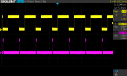
Attached...
Tx (w/ processing) and Rx Duty cycles for 2 samples at a time and 8 samples at a time.
It works surprisingly well and without any processing it becomes a FIFO'd resampler effectively. Different sample rates don't matter, everything will be locked to the particular output Hz and clock. I'm sure if given a full audiophile analysis it will suffer some jitter when crossing clocks/fs domains.
In the Rx FIFO FULL interrupt(s), you shift the contents into a temporary space ( you could call it a buffer ).
In the Tx FIFO empty interrupt you shift the contents of the buffer into the FIFO.*
FIFOs and "Buffers", anything from 2 samples to 8 samples work. It makes surprisingly little difference in performance. If you have multiple inputs or outputs, there is plenty of time to loop around them and pick up and mix the Rx buffers before transmitting them.
I got round to quantifying it today with a scope. (Not audio, although there were some sanity tests). Rather the duty cycles of the Rx and Tx interrupts. If it's just routing and mixing I'd be sure you'd be able to max out the SAI blocks with a total of 7 or 8 IO channels of various/mixed rates/formats. I however want EQ too, in fact I want 2 independent EQ channels and that's where the limitations of even a substantial, non ASIC, CPU core comes to bite.
To run 6 peak filters (used for testing as available), is it maxed out. 70% Tx duty cycle running the EQ. Push it a little more and it drops to 1/2 rate. Thats with a single 16bit Extended 48K source and output. If I add a 7th filter it drops to 24K. 🙁
I can tweak and I can fiddle and I can optimise. I can convert the basic IIR peak filters to ARM DSP optimised BiQuads even.
Bottom line. If 6 peak filters on a single 48K stream is MAX, then no amount of optimisation is going to get me twice the EQ channels at 96K, 4 times the performance.
Thoughts?
* Moving the interrupts around from FIFO Empty to FIFO 1/4 full, 1/2 full or even 3/4 full (and blocking while its full) does change the cadence and alignment with the Rx interrupts, but doesn't change the outcome or performance. There are many more combinations to try, so I'm not done yet.
Attached...
Tx (w/ processing) and Rx Duty cycles for 2 samples at a time and 8 samples at a time.
Attachments

Last edited:
I should point out that just literally moving the contents of the Rx register directly into the Tx register works just as effectively. However you lose the ability to upsample then as the FIFO is consumed in the receiver.
There is every potential as well that I find one or more "Doh!" moments in the code where something is done more than once, that doesn't need to be. That happens when you write enough code day to day.
There is every potential as well that I find one or more "Doh!" moments in the code where something is done more than once, that doesn't need to be. That happens when you write enough code day to day.
Last edited:
So I spoke too soon.
Building the code with -O3 or -Ofast and the duty cycle comes down from 68% to 21%.
Will redo the performance limit tests later, but a quick and dirty prelim looks like 2 channels of EQ, a 5 band and a 3 band do look possible. Even at 96K. Also need to see how many of the SAI blocks can be used for inputs as well and not bust the budget.
The SAI FIFOs are actually 8 word. Not 8 byte. The I2S FIFOs are 8 bytes, but SAI 8 words. So in a 32bit frame you get 2 stereo pairs in the FIFO. 4 Samples. That puts the latency in the realm of 2 digit microseconds. Not bad for a bit of hobby code and a £13 MCU.
You may want to have a look at: https://www.diyaudio.com/community/threads/uac2-i2s-input-on-stm32f723e-disco.393702/#post-7237557 - I'm using the DISCO board for the F7 and it seems fine.
It sounds like you're implementing a IIR/FIR on the data stream. You will need some buffer windowing to allow the FIR to sample.
The real question is - how good is the H7's output clock? Given the SAI interface is derived from the internal clock. You could gate the output using a output clock and feed the clock into the SAI interface for better performance.
Just remember the H7 has multiple peripheral matrices, and DMA can't go through the matrix-to-matrix bridges.
The IIR filters contain their own (previous N sample) buffers, although it is noted they need to be made stereo aware or their state structs duplicated for L and R. Otherwise I'll get filter cross talk.
So. There is no DMA. No buffers. It literally processes each sample in turn, if you desired. I find 4 at a time works slightly better, the timing on 1 sample at a time was a bit hit and miss before optimisation.
On clocks. Firstly the clocks between streams are uncoupled. The FIFO contents are effectively "held", like as in "sample and hold" like in an ADC. The data there in is changed in the receive interrupt which is non-interruptible by the Tx interrupt. So it doesn't really matter when the FIFO contents get written or read, the timing of each can be completely different and it will do something sensible. Exactly, to my understanding how a resample IC works.
The practical aspects presented by this are somewhat more complicated, especially when you introduce SAI synchronisation mechanics.
The H7 only has a single external master clock in. The only issue with that is... all my sources except 1 are Master and each beat to their own master clock.
Remains to be seen how much this actually bothers it, but as the master clock is only really there (in STM32) as a super sampler rate for the bit clock and I already have timing decoupled ... I am going to pick one input clock and use it as the master clock through out.
On the inputs and output. SAI allows you to lock blocks together as slaves of each other. For my dual output, for example in this prototype the second output only has a "Data" line. It shares it's clock and LRstrobe from the other output. It also means I don't need to interrupt on individual outputs either, I can just write both outputs in the same Tx interrupt as they are completely in sync.
I did find it fairly easy to get a 0% drift with the internal clocks, when you have 480Mhz SysClk it's fairly easy to get PLLs for 48k/96k etc.
On resampling and drift. During torturing the thing with various loads, I have found it resampling at rates I didn't know existed and the PCM5102 seemed happy enough to carry on playing. Sample rates like 32Khz. Or 64Khz. I'm sure the PCM5102 id doing it's damnest to clean that up using it's own FIFOs.
EDIT: I know I'm preaching to the choir, but as you know, unlike in a RaspberryPI or other "big iron" with a "general purpose os", on an MCU if your timing is working with 100ns timing margin.... it will stay working at that timing margin. Nobody interrupts your core to load a 3Mb JPEG. The core is all yours and you can literally count you CPU cycles.
To give you an idea of how simple this actually is, here is current core of the code.
Code:
void SAI_Tx_Interrupt(SAI_HandleTypeDef *hsai) {
    /* Currently 4 16bit samples in 32 bit words */
    // Mix
    for( int i=0; i<4; i++) {
        tx1Buffer[i] = rx1Buffer[i];
        // tx1Buffer[i] += rx2Buffer[i];
    }

    EQ_Run(tx1Buffer);

    for( int i=0; i<4; i++) {
        // Just in case.  Not really required.  Anti glitch.
        while( (hsai->Instance->SR & SAI_xSR_FLVL)>>16  == 7) {
        }
        hsai->Instance->DR = tx1Buffer[i];
    }
    __NOP();
}

void SAI_Rx_Interrupt(SAI_HandleTypeDef *hsai) {
    /* Currently 4 16bit samples in 32 bit words */
    for( int i=0; i<4; i++) {
        // Just in case.  Not really required.  Anti glitch.
        while( (hsai->Instance->SR & SAI_xSR_FLVL)>>16  == 0) {
        }
        rx1Buffer[i] = hsai->Instance->DR;
    }
    __NOP();  // for breakpoint
}I took at look at the 550Mhz dual core H7/F7s. The top of the line, a 767 I think has a 550Mhz M7 and a 240Mhz M4. That 240Mhz M4 core would work absolutely perfectly as a mixdown thread concurrently with the Tx thread running the EQ.
The trouble is... finding them.
I am already off loading all additional features to another MCU. Stuff like the TFT GUI screen. Also another MCU doing nothing but handling 6 rotary encoders. Gotta love SPI interrupt struct transfer.
The trouble is... finding them.
I am already off loading all additional features to another MCU. Stuff like the TFT GUI screen. Also another MCU doing nothing but handling 6 rotary encoders. Gotta love SPI interrupt struct transfer.
The H7 only has a single external master clock in.
The SAI has an interface can take an external clock (at least in the F7). That can then drive the FIFO and output. If you really want to be accurate you could simply run a FIFO on the output and clock that in hardware at the same time (for clock leading edge etc).
The STM will quite happily run as it feels like, the issue is how accurate would the down stream DAC be given it's using the STM's bit clock output.
HINT: the scope's internal clock that you're measuring using may not be up to the task with higher bit rates. At 24MHz, and a 200MHz scope the scope's own clock jitter should be understood..
So we are on the same page on clocks.
Master clock - usually high MHz range used to derive the bit clock on a master or super sample the bit clock on a slave.
Bit clock - drives the sampling of the data line.
LRClock (slot strobe whatever) - synchronises the L/R data bytes, or multi-slot TDM-like multichannel streams. (I figure if you are worried about sample timing accuracy it is this clock you want to pay attention to. The transition of this clock triggers the actual DAC operation for the sample. Luckily it's one of the slowest clocks in the setup = sample rate (*slots/2)
My understanding is there is a single SAI / I2s external master clock. There may be separate PLL inputs (generated or derived) for SAI1+2 and different ones for SAI3+4, but ultimately there is only 1 external master clock input. So you could, maybe use an external clock for some streams and a generated PLL clock for others.... not sure why though.
You can have up to, I think 4 Async masters receiving bit clock, but not 4 receiving a master clock. I do not know the practicallities of using a GPIO line or "Clock in" like to facilitate multiple master clock ins.
I haven't done anything in a particular on testing accuracy.
I mean I have been scoping the timing signals and I2S signals and when I do the trigger Hz is usually "as expected" down to the 4th decimal place.
For example, things like 96.0001kHz and things like that. Which is honestly probably probably "in the noise" anyway. I don't know if the scope measures Hz that accurately.
I suppose one test is a clock counter over several hours, work out the total drift of the mathematical absolute. That would find the drift rate. Finding the jitter rate could be more tricky.
I could get it into a state of jittering obviously by overloading it, right on the cusp, if you will and the LR clock and timing would start to jump around, say 48.0001kHz, then 47.895kHz then 48.6521kHz and so on.
You can use the internal divider/multiplier system with the input clock and the SAI can use that as the clocking device, or, you can use an external input as a bit clock. Having a high master clock and a PLL with a divider will improve accuracy. The question is how much?
I use an external clock to operate the ADC, that then drives the bit clock into the STM SAI interface at 24.576MHz. It's possible to do the same with the DAC and therefore reduce phase noise etc.
Don't worry about it - that sort of thing can be retrofitted if it's found to be an issue by adding an external clock.
The only way I can see phase noise at that rate is to use the ADC and look at the output change (lowering noise floor and peaks have a narrower base). The SDS1104 seems to show some of it but after that, it's own clock isn't perfect enough. All depends on what how much you want to accept.
I keep wondering... If you had a master xtal at 24.576Mhz and elsewhere you removed the xtal from a "master source" like an ADC and replaced it either with the bare clock signal ... or replaced it with a suitable ceramic resonator and drive it from the other master clock.... could you force sync 2 master inputs together?
The other thing I'm wonderig, I'll through in, in the off chance you have stumbled upon it... How to use the tightly coulpled core memory (DTCM?) in the H7. As I'm only using a few hundred bytes of RAM it would make sense to put it in the tightly coupled RAM. I thought it was just a compiler/linker directive on the declaration, but my googlings kept revealing complicated custom linker scripts and what not.
The other thing I'm wonderig, I'll through in, in the off chance you have stumbled upon it... How to use the tightly coulpled core memory (DTCM?) in the H7. As I'm only using a few hundred bytes of RAM it would make sense to put it in the tightly coupled RAM. I thought it was just a compiler/linker directive on the declaration, but my googlings kept revealing complicated custom linker scripts and what not.
In terms of external clocks, I have the following choices.

or

Excuse the dust crud, macro images always reveal your dust and cat fur 🙂
or
Excuse the dust crud, macro images always reveal your dust and cat fur 🙂
I keep wondering... If you had a master xtal at 24.576Mhz and elsewhere you removed the xtal from a "master source" like an ADC and replaced it either with the bare clock signal ... or replaced it with a suitable ceramic resonator and drive it from the other master clock.... could you force sync 2 master inputs together?
The other thing I'm wonderig, I'll through in, in the off chance you have stumbled upon it... How to use the tightly coulpled core memory (DTCM?) in the H7. As I'm only using a few hundred bytes of RAM it would make sense to put it in the tightly coupled RAM. I thought it was just a compiler/linker directive on the declaration, but my googlings kept revealing complicated custom linker scripts and what not.
You can play with the compiler and bootloader config to change the memory map where variables (and specific variables) are stored but careful of the stack and access restrictions (bit of a rabbit hole to disappear down).
I learnt the hard way that oscilators/clocks are delicate. I destroyed my CCHD-957-20 by simply using a scope probe on the output (an active probe, correct impedance matching and capacitive loading needs to be correct).
Sort out the software & stm first then worry about the clock.
Sort out the software & stm first then worry about the clock.
I have no idea what I'm doing, but I recalled a scope mode that can be used to at least visualise waveform anomolies.
It's using the persist and colour grade. Colour grades by frequency density. The more waves cross a path the redder it gets. Kind of a waveform noise "hot spot" map. The persistence is over 30 seconds. After a few minutes it doesn't look much different from the second image. So there is rising and falling jitter of around 7.2ns. (f~=130Mhz) I have no idea if that's good or bad 🙂
This is not characterising the jitter, just I found it interesting.
The bitclock (obviously)
EDIT: The ringing I'm not so much worried about. It's not that bad really (although I have the bandwidth limiter on, so you aren't seeing the rest of the noise on it!) and the ringing, overshoot, undershoot will be greatly reduced when I move off the breadboard onto PCB with termination resistors and ground planes.

And..... the jitter...?

It's using the persist and colour grade. Colour grades by frequency density. The more waves cross a path the redder it gets. Kind of a waveform noise "hot spot" map. The persistence is over 30 seconds. After a few minutes it doesn't look much different from the second image. So there is rising and falling jitter of around 7.2ns. (f~=130Mhz) I have no idea if that's good or bad 🙂
This is not characterising the jitter, just I found it interesting.
The bitclock (obviously)
EDIT: The ringing I'm not so much worried about. It's not that bad really (although I have the bandwidth limiter on, so you aren't seeing the rest of the noise on it!) and the ringing, overshoot, undershoot will be greatly reduced when I move off the breadboard onto PCB with termination resistors and ground planes.
And..... the jitter...?
Last edited:
So you don't need to worry too much about the wave form top but as long as the triggering at 20% and 80% (or whatever is defined) as logic high and low is correct. A misshaped waveform MAY indicate an overloaded oscillator that will end up with failure.
Here's a shot of my ADC in operation:

So you can see it's bad.. but you can see that the noise isn't causing bit errors.
Here's a shot of my ADC in operation:
So you can see it's bad.. but you can see that the noise isn't causing bit errors.
The figure I tend to look at is the total peak to peak voltage and compare it to the 3.3V or 5V CMOS/TTL pins and what they will tolerate. Note. They will tolerate a lot more than would be good for them. It will shorten their lives. A lot of that overvoltage is going through the ESD diodes and zenner protection circuits if they exist. I'm sure it does them no good.
I have seen UARTs ringing on breadboards to a total of 9VPP... on a 3.3V circuit. All manor of solution exist depending on how much you want to throw at it. I like to start with some 100 ohm resistors. They tend to limit the current, so the inductive fields don't get as excited in the cables/traces. Or at least that's my pigeon electronics for it.
The optical board I'm using has an HC74 series line driver IC... I think that's overkill, but might explain my ringing being minimal. ?
So I tested the synchronised SAI outputs. Worked perfectly. Setup the other slave transmitter block and bluntly copied the stream into it... Hooked up the spare dac and .. two outputs. Only a single extra pin on the MCU
Yes - the peak should be within their tolerance. However from a logic perspective it's the transition across the low and high voltage (which is about 20% and 80% to allow for noise) and the timing of that transition that is important.
Also dangerous is reflections from non-matched impedance that causes a spike to peak over the top of the tolerance - this is what I believe happened using my probes on my oscillator.
A shunt regulator or a series regulator should cope with outputting 3.3V from 5-9V and burn the excess energy as heat.
- Home
- Source & Line
- Digital Line Level
- STM32H7 Dual Software EQ - so close, but so far.