Idea:
Opamp input stage, followed by a voltage stage gain to get rail to rail swing for the signal so I can ditch the STK unobtainium. I am clearly working above my pay grade here, but I feel like I should be able to figure this out, and hopefully learn a lot in the process. If I'm way out of my element, please let me know.
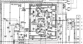
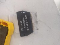
I acquired a broken Yamaha r2000, with a toasted STK3156 Voltage Amplifier chip. I got another one, and the cheap Chinese crap failed. So rather than hunt endlessly for another genuine STK, I would like to replace it with something more fun. Since I have the Yamaha schematic with voltages at different pins for the STK, it seems plausible that I should be able to figure this out. I could not find a datasheet for the STK3156. With the Yamaha schematic, I see two positive power supply pins, and 2 negative voltage supply pins. One each +-20V, and one each +-86V. I suspect that the +-20V supply at pins 9 and 10 is providing the voltage for the initial input stage of the amplifier, and then there is a voltage amplification stage that is supplied by +-86V at pins 7 and 8. These are Vcc and Vee used to bump up the signal voltage. Output to the power stage is from pins 3 and 5.
Basic idea is, can I take the input signal and run it through an opamp, and then build a voltage gain stage to bring the potential swing of the signal up to the rails. An opamp is compact, and I’m not averse to using to them. Then the voltage boosted signal can pass to the power amplifier section of the amp normally. I could place all this on prototyping pcb board, and stick it in the STK slot. Bam problem solved. The bias for the power output is on the power amp board, as is the xprocessor that decides to use the high voltage 86V rail (+-B on the schematic) or the low voltage 46V rail (+-B1).
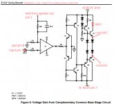
So the Voltage amp stage after the op amp would want to be able to swing the signal to +-86V (or close). I would need a circuit for each channel that could do something like the attached schematic. (snagged it from TI website, paper attached.)
Would something like this work at all? Original schematic shows it going to an inverted input, but if I am taking a single output from the opamp, and sending it to the VAS, it shouldn’t matter…. Right? Do I need to add a compensation cap at q3 and q4? Do I just need to go back to school?
Input is coming from the attenuator (volume knob.) I am unsure how to calculate the voltage gain at each step, in order to determine the voltage gain at each stage, to get the output close to the rails. Help would be appreciated. This is my most ambitious modification to a stereo idea to date.
Thanks for any help.
Opamp input stage, followed by a voltage stage gain to get rail to rail swing for the signal so I can ditch the STK unobtainium. I am clearly working above my pay grade here, but I feel like I should be able to figure this out, and hopefully learn a lot in the process. If I'm way out of my element, please let me know.
I acquired a broken Yamaha r2000, with a toasted STK3156 Voltage Amplifier chip. I got another one, and the cheap Chinese crap failed. So rather than hunt endlessly for another genuine STK, I would like to replace it with something more fun. Since I have the Yamaha schematic with voltages at different pins for the STK, it seems plausible that I should be able to figure this out. I could not find a datasheet for the STK3156. With the Yamaha schematic, I see two positive power supply pins, and 2 negative voltage supply pins. One each +-20V, and one each +-86V. I suspect that the +-20V supply at pins 9 and 10 is providing the voltage for the initial input stage of the amplifier, and then there is a voltage amplification stage that is supplied by +-86V at pins 7 and 8. These are Vcc and Vee used to bump up the signal voltage. Output to the power stage is from pins 3 and 5.
Basic idea is, can I take the input signal and run it through an opamp, and then build a voltage gain stage to bring the potential swing of the signal up to the rails. An opamp is compact, and I’m not averse to using to them. Then the voltage boosted signal can pass to the power amplifier section of the amp normally. I could place all this on prototyping pcb board, and stick it in the STK slot. Bam problem solved. The bias for the power output is on the power amp board, as is the xprocessor that decides to use the high voltage 86V rail (+-B on the schematic) or the low voltage 46V rail (+-B1).
So the Voltage amp stage after the op amp would want to be able to swing the signal to +-86V (or close). I would need a circuit for each channel that could do something like the attached schematic. (snagged it from TI website, paper attached.)
Would something like this work at all? Original schematic shows it going to an inverted input, but if I am taking a single output from the opamp, and sending it to the VAS, it shouldn’t matter…. Right? Do I need to add a compensation cap at q3 and q4? Do I just need to go back to school?
Input is coming from the attenuator (volume knob.) I am unsure how to calculate the voltage gain at each step, in order to determine the voltage gain at each stage, to get the output close to the rails. Help would be appreciated. This is my most ambitious modification to a stereo idea to date.
Thanks for any help.
Attachments
Well, I doubt you need +- 86 v swing to drive the output stage. If it could supply the current, 86 vpp is 60 vaverage, which into 8 ohms is 453 watts. With a single pair of output transistors, this looks like a 50 to 60 W amp. You probably need +-3 v swing into current followers tr704 tr705.
If I were doing it, I would use a LM675 op amp in a TO220 package. It can use a +-30 v supply max. I doubt if you need that much, your +-20 should do the job. Will supply up to 3 amps out. Put a big heat sink on it.
Set it up for ~gain 10, Rf/rin =10. Simple inverting op amp. If the TI datasheet doesn't show it, This website should have it: Op-Amp Adder and Subtractor - Linear Integrated Circuits - Wikitechy
I'd build this on 1/16" NEMA CE material I buy from mcmaster.com and saw up into rectangles. If you don't mind paying $10 for the predrilled holes, vector board from newark/digikey/mouser works. Don't for get high freq killer 33 pf cap around the feedback resistor, and protect the input with 68 to 100 pf from + to - input to reduce rf interferance.
Last edited:
Yeah, 450 is not right. Haha. The amp for this receiver is rated at 150wpc @8 ohm.
Why would there be a +-86v supply to the stk then? I thought the voltage amp section was supposed to increase the signal at max output close to the rail voltages. Am I confused? The schematic does show the output voltages at +-2.5v or so, it sounds like you are on target. I couldn't figure out from the service manual what condition that voltage is generated at.
That particular opamp would simplify the opamp supplies... To use something like an lm4562 would require me to get the opamp supplies down to +-15v or so.
The x processor allows the use of the 86v rail for very high power bursts. Most of the time the amp runs on the 46v rails if I understand correctly.
I'll modify my schematic to include an input cap.
Thanks!
Volume to TR704 705 is all current, not voltage swing. the voltage swing happens at the output transistors. +-86 is pretty extreme for a 150 w/ch amp, these days would be about +-65 or so with higher gain transistors.
My first cut design leaves out all feedback from the output to the op amp input. This should get you under 1% hd, but for more accurate sound you'll have to provide feedback from the output to the op amp input. Make sure it is negative feedback, which means if the output stage inverts the feedback has to go to the op amp + input. I'd try a 6.8k resistor first try for global feedback.
Another possible quibble, the phase of the surviving channel with a good stk module should be the same as this channel. So you may have to fool with a non-inverting LM675 circuit (which is more parts) if that is what you need.
Oh, to be specific, q3,4,5,6,7,8 aren't needed with a LM675. You do need feed back resistor from output of op amp to negative input to limit the voltage gain to 10 or so.
Last edited:
Thanks for responding. I do appreciate it. I am confused. I thought TR704 through 709 were all emitter followers, and as such, provide nearly unity voltage gain (little to none), but do provide high current, and as such add the power to the higher voltage signal. Therefore the voltage gain would need to come before arriving at tr704 and tr705. The toasted stk even says voltage amplifier on it. So I thought all the voltage gain was done first, in the stk, and then power was added at the current gain stage.
Attachments
Well, yeah, but the LM675 can do both voltage gain and current gain up to 3 amps. If the input is 1.6 vac (nominal line level) then 10x gain would get you 16 vac out. If you more, change feedback resistor and go 20x gain, for 32 v out. 32 is 128 watts into 8 ohms. Go for 21x gain for 150 w.
Actually you cant get more voltage out of the LM675 than the rails. So with +- 20 rails you could only get 36v pp out. (+-18) .7x36 vpp is 25.6 vaverage? Still a lot of wattage. with 30 v rails you could get maybe +-56 vpp out.
Actually you cant get more voltage out of the LM675 than the rails. So with +- 20 rails you could only get 36v pp out. (+-18) .7x36 vpp is 25.6 vaverage? Still a lot of wattage. with 30 v rails you could get maybe +-56 vpp out.
Last edited:
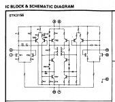
Deeper digging inn the service manual revealed the stk3156 block diagram. The 20v are rails for initial differential input, then it uses the 86v as rails for a second differential pair, and finally, 86v for voltage gain. Check it out.
Attachments
So the stk3156 is an op amp that can operate on +-86. you can't buy that anymore.
The plus and minus inputs of the power section are about 4 to 6 diode drops between the two points. For minimum distortion you need to provide two inputs, about 2.4 or 3 volts apart from each other. This can be done with a diode stack pulled up & down by resistors from the same rails as the LM675, or by a Vbe multiplier (transistor) between the same two resistors. As the differential voltage between inputs should decrease as the transistors in the power board heat up, the diode stack or the Vbe multiplier should be mounted & thermally coupled to the output transistor heat sink.
The size of the two resistors pulling up & down the diode stack/vbe multiplier should be large enough to exceed maximum current limits of the LM675, also to not heat it up unduly.
Try to adapt the following schemes:
DLH Amplifier: The trilogy with PLH and JLH amps
Mr Evil's Realm - Rush Cascode Input Stage
Leave Tr1, Tr2, Tr4, Tr9. Collectors Tr4, Tr9 to connect with the Yamaha amplifier. In collectors Tr1, Tr2 include cascode for 20 century. 4QD-TEC: Low distortion Audio amplifier
DLH Amplifier: The trilogy with PLH and JLH amps
Mr Evil's Realm - Rush Cascode Input Stage
Leave Tr1, Tr2, Tr4, Tr9. Collectors Tr4, Tr9 to connect with the Yamaha amplifier. In collectors Tr1, Tr2 include cascode for 20 century. 4QD-TEC: Low distortion Audio amplifier
Last edited:
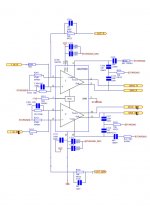
I just got my hands on a busted arcam avr600. A little investigation leads me to believe that it would be very difficult to fix. So I gutted it, and will be building a honey badger in the case. BUT that relates to this, because the arcam uses TI LM4702C opamps for the input and voltage gain stage of the amp. And while it is using +-59V rails, the lm4702C can handle up to 200V supplies, according to the data sheet, but is happier closer to +-75V. A and B variations are happier a little higher, but C is what I have. I have several of the C variant chips from the arcam, so I may see if I can mock something like the circuit below up on a proto board.
This would allow for the use of the original drivers and output stage as designed by Yamaha, and allow the use of the xprocessor to use the higher power rail when called for, as per the original design.
If I am mistaken somewhere, please let me know. But, with several lm4702C in hand, I am leaning that direction. See the attached circuit and I have included a link to the TI lm4702 sheet documenting using the chip to drive output stages, and discrete driver stages, as well as it's integration with resistor based bias stage (which the r2000 also has on the power board).
TI lm4702 article.
https://www.ti.com/lit/an/snaa045a/snaa045a.pdf
Attachments
Last edited:
Oh, wow, LM4702 is a unicorn.
C revision is listed by TI as +-75 max. You might get away with +-82 for a while, but at your own risk.
digikey is listing these for sale, but actually from Rochester surplus house, with their standard $250 minimum. If you can use 28 of them they will let you have them for $9 apiece + freight.
You can download the LM4702 datasheet from digikey after you pull up the part.
I don't know if all that voltage swing is necessary for the input amp. Peavey PV-1.3k that I own has a triple emmiter follower output like your yamaha. +-85 v supplies. They drive all that with a single 4558 op amp (through a diode stack like in post 8) running off +-16v supplies. It puts out 650 w/ch into 4 ohms. You can download the schematic from eserviceinfo.com for free. The difference between the PV-1.3k and the r2000, the peavey has 5 pairs MJ15024/25 output transistor to move all that current. Looks like the r2000 has one pair 2sa968/2sc2774 output transistor.
Warning the power supply for the LM4558 in the Peavey is regulated down from the +-85 (with zeners) because the power supply swings around with the OT collectors, 2 windings in the transformer to allow 2 channels to have separate outputs. Don't know if the yamaha has that feature.
Last edited:
I've reviewed the datasheet pretty carefully, and it states that maximum operating supply voltage is 200v. So with 85v rails, the c revision is below the maximum rated supply voltage by 30v. For the first go around, it may be safe to use the lower voltage supply pins and see if the circuit actually works. Then I can bump it up to 85v and see what happens...
The datsheet does state that the detailed performance specs are guaranteed under the rated +-75v supplies. Above that, but below max rating, device should behave like it does under 75v. I have three of these things. My proto board arrived in the mail yesterday.
I'm a slacker though and I really need to work on my taxes. ☹️
But I think I am on the right track for replacing the stupid stk chip. I appreciate the input so far indianajo. I'm learning, and I feel like my understanding is moving the right direction.
More specifically, does the general circuit layout look pretty good?
I now think that the 4702 might be a straight drop in as long as I get the pins matched up and skip the 20v supply,. (which is only used for the input ltp in the stk anyways.
I don't have all the bits to put the power amp section together yet. But they are coming.
I don't have all the bits to put the power amp section together yet. But they are coming.
A serious question is, does the power supply of the yamaha r2000 have one +-84 transformer winding for both channels, or two. If two you can copy the PV-1.3k circuit pretty directly if the LM4702 doesn't work out. You can leave out the extra op amps that drive the line level echo, the DDT circuits, the LED drive circuits, and the VI limiter transistors, but the op amp, predriver transistors, driver transistors, output transistors are pretty exactly what you are building. Just not as many output transistors, which limits you to 150 w/ch.
I have my doubts about the LM4702, these high gain amp chips are very sensitive to layout. I tried to build a LM1875 amp point to point, it motorboated inexorably on both channels. I believe because the power wires were too long. TI provides a layout for prototype board on the LM4702 datasheet, and my guess is these have to be followed exactly. Getting from the LM4702 output to the r2000 power drive section, and getting the feedback from speaker to minus input, may allow for longer wires.
I have my doubts about the LM4702, these high gain amp chips are very sensitive to layout. I tried to build a LM1875 amp point to point, it motorboated inexorably on both channels. I believe because the power wires were too long. TI provides a layout for prototype board on the LM4702 datasheet, and my guess is these have to be followed exactly. Getting from the LM4702 output to the r2000 power drive section, and getting the feedback from speaker to minus input, may allow for longer wires.
Last edited:
Supposedly early models had stk3106, but it wasn't up to the task, so later models came with the stk3156. Which also wasn't really up to the task. I can't get the damn lm4702 out of the arcam boards. Ruined two of em. Kind of what to leave the other two in the amp board they are in for another project.
dear indianajo, sorry for this message, my English is not good to understand all, so please consider this as a question hoping for your kind advises form your experience. I see that in the past (about 2 years ago) you have faced the problem of restoring the STK Processor Voltage amplifier for the amply Yamaha R2000. I'm tryng to restore an old Yamaha R1000 amply, that has the Yamaha STK7100 processor Voltage power amplifier that, depending on the level of the audio signal, changes the Voltage polarization for the main Amply transistors form +40 0 -40 VDC to +73 0 -73 VDC. Actually it is broken and provide -70 0 +40 ;-). As far as your experience, have you maybe found an equivalent STK processor that could be used in the place of the original yamaha STK7100? I.e. the Sanyo STK 3106 or 3156 could be the right ones? And in the positive case have you already mapped the pin connection to keep the original Yamaha R1000 amply performance? Thank you very much for any your kind reply or advice or some other reference or contact person!A serious question is, does the power supply of the yamaha r2000 have one +-84 transformer winding for both channels, or two. If two you can copy the PV-1.3k circuit pretty directly if the LM4702 doesn't work out. You can leave out the extra op amps that drive the line level echo, the DDT circuits, the LED drive circuits, and the VI limiter transistors, but the op amp, predriver transistors, driver transistors, output transistors are pretty exactly what you are building. Just not as many output transistors, which limits you to 150 w/ch.
I have my doubts about the LM4702, these high gain amp chips are very sensitive to layout. I tried to build a LM1875 amp point to point, it motorboated inexorably on both channels. I believe because the power wires were too long. TI provides a layout for prototype board on the LM4702 datasheet, and my guess is these have to be followed exactly. Getting from the LM4702 output to the r2000 power drive section, and getting the feedback from speaker to minus input, may allow for longer wires.
The production of high power class AB IC's is being rapidly eliminated. The IC manufacturers want everybody to buy class D. The PA manufacturers are happy to sell you amps that are designed to fail in 5000 full power hours. They get another sale in 3-5 years.
I'm resisting but my amps only require 20 ma source/sink IC's. After that they are tiples, two stages of discrete transistor VAS before final emitter followers. Suggest you buy another amp of that design. Typically QSC, Crown, Peavey. Used ones with actual transformers are rather inexpensive, as road bands don't want to carry an appliance that weighs 40 kg.
I'm resisting but my amps only require 20 ma source/sink IC's. After that they are tiples, two stages of discrete transistor VAS before final emitter followers. Suggest you buy another amp of that design. Typically QSC, Crown, Peavey. Used ones with actual transformers are rather inexpensive, as road bands don't want to carry an appliance that weighs 40 kg.
- Home
- Amplifiers
- Solid State
- stk3156 replace with opamp and VAS?