What Tom said in post #2.
It might be boring for you but everything lm3886 has been done, sort of.
Check out the link Tom gave. It's all in there, incl. Layout,
Unless you wanna go another route circuit-wise.
I ended up getting exactly those PCBs and they are very nicely done.
It might be boring for you but everything lm3886 has been done, sort of.
Check out the link Tom gave. It's all in there, incl. Layout,
Unless you wanna go another route circuit-wise.
I ended up getting exactly those PCBs and they are very nicely done.
Hello there
I appreciate what you are saying. There is certainly know doubt about the quality of Toms boards and the fact that everything that can be done has been done as regards the LM3886 circuit design.
But for myself I enjoy fabricating my own boards and muddling through the intricacies of layout to end up with something that works well. Whether it is better or worse than any other design will be down to what my ears receive once the speakers are built.
Visaton FRS8 2004 8ohm speakers in a cyburgs needle. Is the end test scenario.
Regards
AC
Totally understand, ac.
Making something from scratch, mistakes and learn from it,
Is quite constructive and rewarding.
Did the same thing with a discrete design but went the other route with the LM-chips and used the open source design straight.
The cyburgs needle is quite a popular design in germany, let us know how you like it.
Hello there
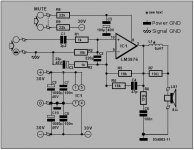
Thanks for the pointers. Having got to this point I think it will be easier to add the components required and tweak the layout to suit the additions. See the attached schematic which my original ‘working’ set up was based on. I think this has all the points you mention above covered.
Regards
AC
That looks pretty reasonable. Don't be afraid of going higher with the gain, the 18k's (or 22k you had originally) are both fine and you can lower the value of the 1k feedback return if you want.
Higher gain can aid stability margins and anecdotally has been said to sound 'better'.
You'll have to determine that yourself 🙂
Hello there
Thanks for the comments gents. Definitely fun to do and somewhat addictive to boot. I will bare in mind the gain settings and play with it I’m sure.
I’ll definitely give a heads up on the end result with the needles. Might be a short delay as Yule looms. Ordered the Chips a week ago. The post has been shocking of late. Seasonally affected of course but CV19 has added to delays. Siiiiigh!
Have a good Christmas all
Regards
AC
Hello there
I hope you all had a joyous Yule.
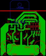
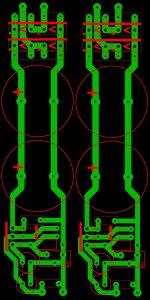
Finished the PCB design. Presented here for roasting. The chip will be mounted flat on the trace side. The board is around 48mm square.
regards
AC
PS Just noticed I haven't traced C6 to ground 😀
I hope you all had a joyous Yule.
Finished the PCB design. Presented here for roasting. The chip will be mounted flat on the trace side. The board is around 48mm square.
regards
AC
PS Just noticed I haven't traced C6 to ground 😀
Attachments

Last edited:
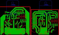
Often true, but this is a VERY SIMPLE schematic and layout.When correctly designed 2 or more sides pcb will improve the amp performances compare to one side pcb.
Extra complication does not provide significant advantage, if at all.
You still need to join top and bottom, so 2 soldered connections per via, that alone takes a lot of the shine out of the idea.
Compared to that, a few wire bridges here and there (IF needed) , are simpler/practical.
Hello there
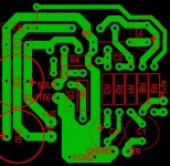
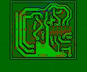
PSU PCB Sorted.
Regards
AC
PSU PCB Sorted.
Regards
AC
Attachments
Last edited:
R6 (Zobel resistor) should be a 2 W type.
I suggest taking the ground for C9 and C10 south to the ground pour instead of all the way to pin 7 and south from there. The largest currents are the charging currents for C9 and C10, so reducing the impedance and "antenna" (loop) area would be good.
It looks like one pin of your input cap is floating when the source is disconnected. I'm generally not a fan of that. I would put something like a 470 kΩ to ground just so the cap doesn't float.
Tom
PCB Revision Bb
Hello there
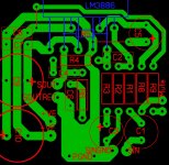
Thanks for the pointers Tom. PCB tweaked as per your guidance. Also made the component outlines reflect the real world to avoid later issues. R6 is the 2W outline but vertical to save space. Do I need a ferrite bead on the long wire lead to avoid rf?
Resistor for grounding the floating input is vertical also.
Regards
AC
Hello there
Thanks for the pointers Tom. PCB tweaked as per your guidance. Also made the component outlines reflect the real world to avoid later issues. R6 is the 2W outline but vertical to save space. Do I need a ferrite bead on the long wire lead to avoid rf?
Resistor for grounding the floating input is vertical also.
Regards
AC
Attachments
- Home
- Amplifiers
- Chip Amps
- Starting again. LM3886 build.