I just purchased and trying to learn my way around Sprint-Layout 6.0. Seems pretty easy to use and similar, but much better to me, than ExpressPCB.
When converting to Gerber files, there are options for SMD solder mask for the top and bottom layers like I have circled below.
Do I select these options only if there are any SMD devices on either side of the board?
Also, are the solder mask offsets at the right set correctly or should they be changed?
These may be dumb questions, but I've never purchased boards with a solder mask before.
Thanks...
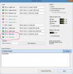
Attachments
When converting to Gerber files, there are options for SMD solder mask for the top and bottom layers like I have circled below.
Do I select these options only if there are any SMD devices on either side of the board?
Also, are the solder mask offsets at the right set correctly or should they be changed?
I don't use this program, but it appears that the solder mask is created in two parts, one part only for SMD, and the other part for all else.
You will need both parts if you have both kinds of footprints, otherwise not. The default offset is fine.
This may be to create the solder paste stencil mask, print out the Gerbers and post them so we can see.
With a mixed technology board (PTH and SMD) the soldermask artwork will have the PTH pads and the SMD pads, your solder paste artwork will have just the SMD pads on it.
These days it is recommended not to oversize or undersize these pads, but create them all 1:1 (in relationship to the copper pad) and let the PCB manufacturer oversize the soldermask pads and the solder paste stencil manufacturer undersize your paste pads if required.
These days it is recommended not to oversize or undersize these pads, but create them all 1:1 (in relationship to the copper pad) and let the PCB manufacturer oversize the soldermask pads and the solder paste stencil manufacturer undersize your paste pads if required.
So no one here uses Sprint-Layout??
FWIW I'm just *starting* to use it now, to replace my stone age era DOS based Autotrax and Tango faithful workhorses for the last 20/22 years , but haven't yet gotten to the soldermask stage.
Still drawing from scratch parts outlines it surprisingly does not have, such as many chipamps which I use daily.
Oh well.
- Status
- Not open for further replies.
- Home
- Design & Build
- Software Tools
- Sprint Layout Solder Mask Questions