I´ve been using Sprint Layout some time but I have one little unclear thing which would be good figured out.
Is there anyone who use Sprint Layout and dealing with "copper pour" function has used "hatched" copper (or hatch fill) pour or - grid? or net? like copper pour - like there:
https://documentation.circuitmaker....9/Pcb_Obj-PolygonPour_Example_HatchedMode.png
If so, then where this function located in Sprint Layout 6.0 and 7.0.
I know that there is solid ground plane function which i can use to fill unneccesary empty areas but i dont find where i can change "solid" to "hatched". I am afraid that Sprint Layout has not this option at all 🙁 ?
The only way that I know how is to draw a "zone", select the zone to show properties, and then check the box that says "hatched". The zone will now be filled with a hatch pattern.
George
George
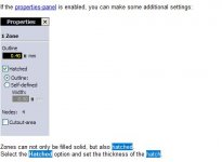
yeah, now i saw this but - how can i go to this box and change "hatched" - i saw that this exist when
1. allow "Propertis" panel
2. select "Zone" to left toolbar
3. I then try do draw zone and I saw that right Properties panel appear "1 Zone" and hatched, nodes, cutout...bla-bla-bla...but how can I go to mark this "Hatched" ???
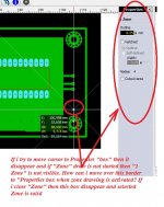
When i draw this "Zone area" then i cant move cursor out of board window - how i can select this Hatched?
1. allow "Propertis" panel
2. select "Zone" to left toolbar
3. I then try do draw zone and I saw that right Properties panel appear "1 Zone" and hatched, nodes, cutout...bla-bla-bla...but how can I go to mark this "Hatched" ???
When i draw this "Zone area" then i cant move cursor out of board window - how i can select this Hatched?
Attachments
Last edited:
You haven't finished drawing your zone. Complete the zone by clicking on your start point. Then you can alter the zones properties on the sidebar.
Thank you all 🙂
This seems so logic thing now. I read some time Sprint Layout Tutorial but dont find this and I read again and again. But thanks to you now it clear.
One question more - can I hatch (auto) ground plane? I try but seems that this "editor" does not work at ground plane? I want to use this grid like fill style because I do all PCB at home and i like it - this seems nicer than solid. I was read too that this type groundplane sometimes its not good but 98% analog electronics I think that there is not problems this grid pouring.
I know that this ground copper pouring works at Mentor PADs but simpler design i dont need use PADs because I have very little knowledges at PADs.
Then - if i can hatch ground plane at Sprint Layout, then how?
And thanks again!
You can't hatch the auto gnd plane or edit it other than place some keep out zones.
For diy etching best to leave solid as the less copper to remove the better.
For diy etching best to leave solid as the less copper to remove the better.
You can't hatch the auto gnd plane or edit it other than place some keep out zones.
For diy etching best to leave solid as the less copper to remove the better.
OK. Thank you.
I think that when i spent some extra time, then i can draw this ground fillings.
Maybe big solid area etching is better when you only get regular etching chemicals but I perform etching another way. I use Hydrochloric acid and Hydrogen peroxide solution bath to etch boards - this is very cheap way when you compared to Ferric chloride or sodium/potassium persulfate method.
Only bad thing that hydrogen peroxide is not allowed some countries, another way I think that this is time saving and very productive (same way like commercial manufacturig) method to etch PCBs.
Ground plane
U can activate copper pour in sprint layout,but not hatched,only plane,press the button near grid capture button and enter a clearance distance value thats all
U can activate copper pour in sprint layout,but not hatched,only plane,press the button near grid capture button and enter a clearance distance value thats all
You can add copper pour in sprint layout but not hatched only plane, just click the ground plane button and enter a clearance value,thats all
- Home
- Design & Build
- Software Tools
- Sprint LAY - how?